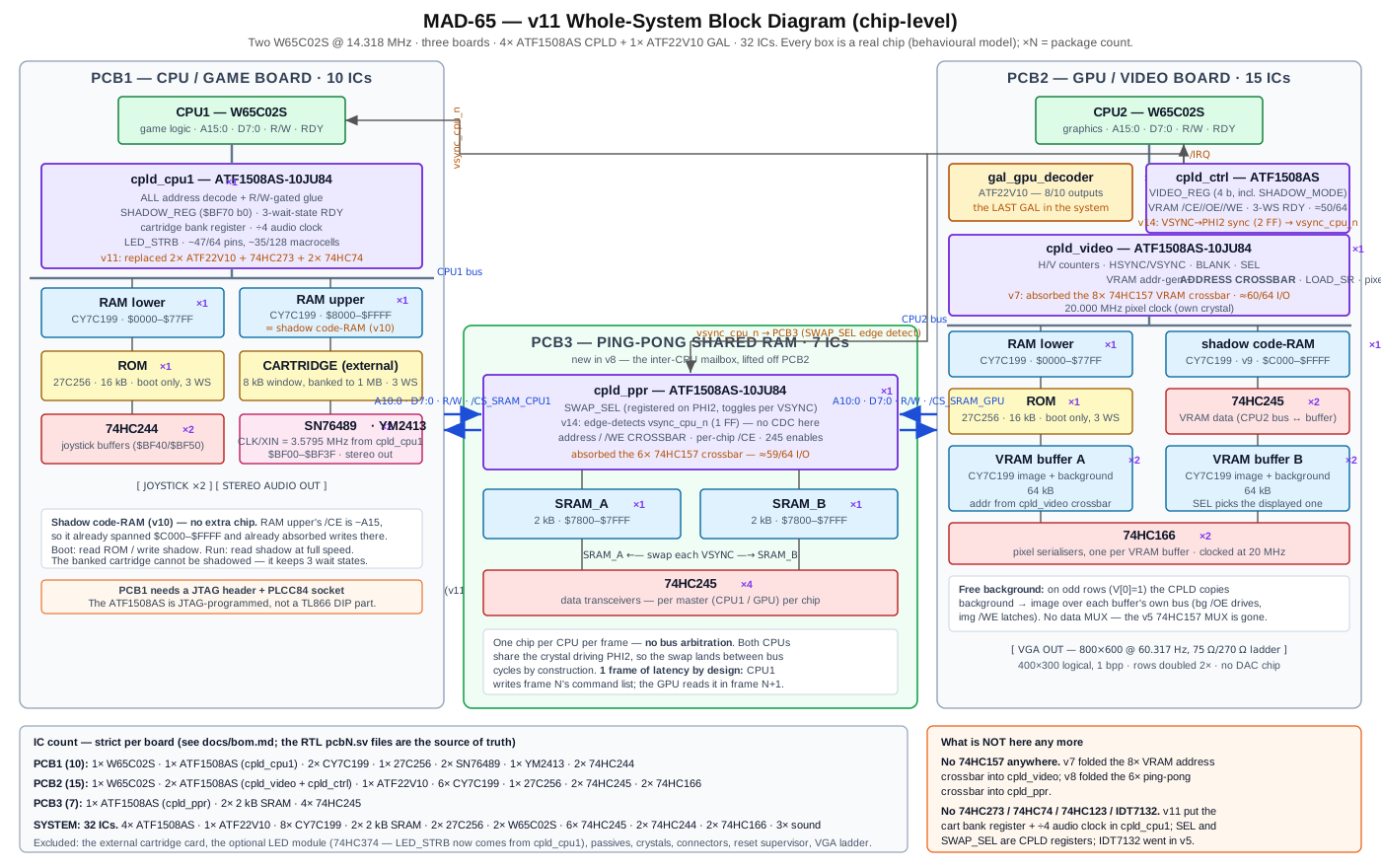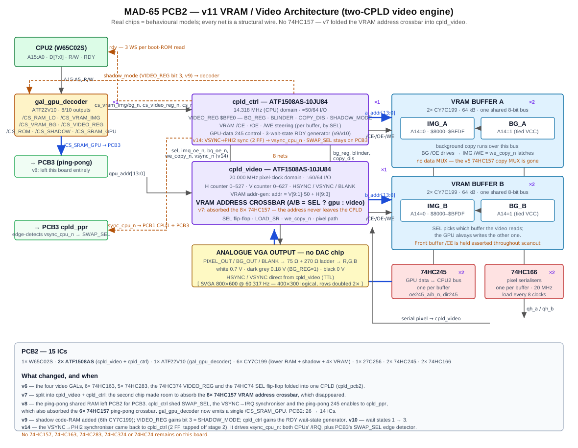
The MAD-65 console is built around two independent 65C02 processors running in parallel. Each has dedicated memory and a clearly defined role. Communication between them uses two 2 kB SRAMs operating in a ping-pong (double-buffer) scheme — one chip per CPU per frame, swapped each VSYNC. Design philosophy: maximum hardware simplicity, minimum component count, hobbyist-friendly (TTL/GAL, through-hole).
cpld_video + cpld_ctrl + cpld_xbar), VGA outcpld_ppr: SWAP_SEL, address crossbar). PCB1 and PCB2 each cable into their own port. v14: the VSYNC→CPU-clock synchroniser moved to PCB2, so this board takes the already-synchronous frame /IRQ and only edge-detects it.A chip-level whole-system diagram is in
MAD65_system_v6_blockdiagram.svg; the PCB2 video/VRAM detail
is in MAD65_video_v6_blockdiagram.svg. ASCII summary:
┌──────────────────────────────────────────────────────────────────┐
│                          MAD-65 CONSOLE                          │
│                                                                  │
│  PCB1 ─────────────────────────┐  PCB2 ────────────────────────┐ │
│  │       CPU1 (main)           │  │       CPU2 (GPU)           │ │
│  │       65C02 @ 14.318 MHz    │  │       65C02 @ 14.318 MHz   │ │
│  │                             │  │                            │ │
│  │  - game logic               │  │  - sprite rendering        │ │
│  │  - joystick handling        │  │  - line drawing            │ │
│  │  - sound control            │  │  - tile rendering          │ │
│  │  - cartridge banking        │  │  - VRAM filling            │ │
│  │                             │  │                            │ │
│  │  RAM:  2× CY7C199-15PC(64kB)│  │  RAM:  1× CY7C199-15PC(32kB)│ │
│  │  ROM:  27C256/AT28C256 16kB │  │  ROM:  27C256/AT28C256 16kB│ │
│  │  CART: banked 8 kB (1 MB)   │  │  VRAM: 4× CY7C199-15PC(128kB)││
│  └────────────┬────────────────┘  └──────────────┬─────────────┘ │
│               │ /CS_SRAM_CPU1                    │               │
│          ┌────┴──────────────────────────────────┴─────┐         │
│          │    PING-PONG SHARED RAM  2× 2kB (PCB2)      │         │
│          │    SRAM_A ←swap→ SRAM_B each VSYNC          │         │
│          │    ($7800–$7FFF both CPUs, 1 frame latency) │         │
│          └─────────────────────────────────────────────┘         │
│                                                                  │
│  PCB1 ─────────────────┐         PCB2 ────────────────────────┐  │
│  │  2× SN76489         │         │   VIDEO CIRCUIT (CPLD)     │  │
│  │  1× YM2413          │         │   400×300 / 800×600 @60Hz  │  │
│  │  stereo mixer       │         │   3× ATF1508AS CPLD        │  │
│  │  [STEREO AUDIO OUT] │         │   + 74HC166/245 glue       │  │
│  │  [JOYSTICK ×2]      │         │   BLINDER + BG_REG         │  │
│  └─────────────────────┘         │   background copy          │  │
│                                  │   [VGA OUT]  [VSYNC IRQ]   │  │
│                                  └────────────────────────────┘  │
└──────────────────────────────────────────────────────────────────┘
                                   IRQ (VSYNC) → CPU1 and CPU2
| Parameter | CPU1 (main) | CPU2 (GPU) |
|---|---|---|
| Model | WDC W65C02S | WDC W65C02S |
| Clock | 14.318 MHz (shared crystal) | 14.318 MHz (shared crystal) |
| RAM | 32 kB (lower) + ~32 kB (upper) | ~30.75 kB lower only ($0000–$77FF) |
| ROM | 16 kB (system/OS/demo) | 16 kB (firmware + graphics routines) |
| Cartridge | yes (8 kB banked, 1 MB max) | no |
| IRQ | VSYNC | VSYNC |
| Role | game logic, I/O | graphics generation |
Clock note: WDC W65C02S is specified up to 14 MHz. The 14.318 MHz crystal (NTSC standard, widely available) is marginally over spec but works. The real memory constraint is the datasheet read window tACC = tCYC − tADS − tDSR ≈ 69.8 − 30 − 10 ≈ **30 ns** (the earlier "≤55 ns" figure dropped the tADS+tDSR terms and is wrong). At 14.318 MHz a single-cycle read therefore needs ≤~30 ns from address-valid to data, i.e. fast (~10–15 ns) SRAM plus a fast decoder — no 45–55 ns parallel ROM/EPROM meets it. All system RAM is CY7C199-15PC (32K×8, 15 ns), comfortably inside that window on its own, so the remaining constraint is purely the EPROM/cartridge. Two mitigations are used, and as of v10 both CPUs use both: each runs its code from a fast shadow code-RAM (GPU: a dedicated 2nd CY7C199-15PC, see §5; CPU1: the existing upper RAM chip, which already covered $C000–$FFFF — see §4), and each slow EPROM read gets three wait states (~239 ns of access time). Because the EPROM is only read during the boot copy, those wait states cost nothing at run time — total boot-to-first-frame is ~215 ms. The one path that keeps its wait states permanently is the cartridge, which is banked and so cannot be shadowed. Other slow-memory read paths similarly want fast SRAM or a wait state at full clock. (Alternatively, halving the CPU clock to 7.159 MHz relaxes the window to ~100 ns and lets slower parts run without wait states.)
Write timing — /WE = !(PHI2 & !R/W) (v16). Reads are the demanding direction, but writes have
their own rule and it is not optional. On the 65xx bus the cycle boundary is PHI2's falling edge:
address and R/W go valid tADS (~30 ns) after it, write data tMDS after it, and all are released
only ~10 ns (tAH/tDHW) after the next falling edge. An async SRAM commits the addressed cell at
the end of the write pulse — the rising edge of /WE — so /WE must be qualified with PHI2 to
place that edge where the data is still valid. Every write strobe in the system now is: each board
CPLD emits one /WE feeding that board's RAM, sound chips, VRAM and its PCB3 port, and cpld_ppr
merely muxes the already-qualified strobes. (The video-side WE_COPY is exempt — it belongs to the
20 MHz pixel-clock domain, not the CPU bus.) Through v15 every /WE was raw R/W, which put the
commit edge ~20 ns after the CPU had stopped driving and, on back-to-back pushes (JSR, IRQ/BRK/NMI),
never released /WE between cycles at all. See the address-decoder doc §3a.
Clock sharing: CPU1 and CPU2 share one 14.318 MHz crystal — signal buffered through 74HC04. Despite the shared clock both CPUs are functionally asynchronous — the ping-pong shared RAM scheme guarantees exclusive access per frame without any arbitration logic. The video circuit has its own independent 20.000 MHz crystal (SVGA pixel clock).
Clock domain crossing (v14): The only cross-domain signal is VSYNC (20 MHz video domain → 14.318 MHz CPU domain), and it is synchronized once, on PCB2 — the board that generates it. cpld_video hands vsync_n to cpld_ctrl over a single on-board CPLD-to-CPLD track; cpld_ctrl clocks it through two flip-flops (VSYNC_S1 → VSYNC_S2) on CLK_14318 and inverts stage 2 into the active-low VSYNC_CPU_N. That one clean, CPU-clock-domain signal goes to all three boards: CPU2's /IRQ locally, CPU1's /IRQ over the connector to PCB1, and PCB3, where cpld_ppr recovers the frame edge with a single flip-flop (VSYNC_CPU_N_D) to toggle the registered SWAP_SEL. So the frame IRQ and the ping-pong swap still derive from one edge detector, and no board other than PCB2 contains a clock-domain crossing. No other CDC issues exist; double-buffered VRAM physically separates the two clock domains.
Why
VSYNC_CPU_Nand notIRQ_N. The net has two different meanings depending on who is reading it. On PCB1 and PCB2 it is genuinely an interrupt request — it wires straight to the CPU's/IRQpin. On PCB3 it is nothing of the sort:cpld_pprnever interrupts anything, it just needs to know where a frame begins. Naming the wire after one consumer's use made the shared-RAM board look like it cared about interrupts.VSYNC_CPU_Nnames what the signal is — VSYNC, re-timed into the CPU clock domain — and leaves each consumer's use to show at the connection point. The_CPUsuffix matchesCLK_CPU/CLK_PIXelsewhere in the design.Why v14 moved it. Through v13 the crossing lived on PCB3: raw VSYNC was cabled from PCB2 to PCB3, synchronized there, and the resulting /IRQ cabled back to both CPUs. PCB3 owns the shared-RAM mailbox, not the video timebase — it was hosting flip-flops on the other boards' behalf, and the round trip meant PCB2 could not raise its own frame interrupt without PCB3 populated and cabled, which is a pointless dependency for video bring-up. v14 also takes /IRQ off sync stage 2 rather than stage 1: the old
IRQ_OUT_N = ~IRQ_S1was effectively a one-flip-flop crossing, so a metastable sample could reach both CPUs' /IRQ pins. The extra stage costs one PHI2 (~70 ns) against a 16.6 ms frame. SWAP_SEL still toggles on the same clock edge as before — v8 spent 2 PHI2 reaching its edge-detect condition and 1 acting on it; v14 spends the first 2 incpld_ctrland the third incpld_ppr. Net wiring change: two backplane signals (vsync_nout to PCB3,irq_out_nback) collapse into one (vsync_cpu_n, PCB2 → PCB1/PCB3), and raw VSYNC no longer leaves PCB2 except to the VGA connector.
$0000–$77FF   RAM        ~30.75 kB  (lower RAM — Zero Page, Stack, game data)
$7800–$7FFF   Shared RAM   2 kB    (Ping-Pong SRAM, active chip for this frame)
$8000–$9FFF   Cartridge    8 kB    (banked window; or RAM when cartridge disabled)
$A000–$BEFF   RAM        ~7.75 kB  (game data, buffers — upper)
$BF00–$BFFF   I/O          256 B   (SN76489 ×2, YM2413, joysticks, cartridge bank register)
$C000–$FFFF   ROM         16 kB    (boot, init, OS API, demo)
Usable RAM: ~38.5 kB with the cartridge enabled (lower ~30.75 kB + upper ~7.75 kB); ~46.5 kB with the cartridge disabled ($8000–$9FFF returns as RAM).
NOT(A15) AND NOT(SRAM_SEL)   → lower RAM ($0000–$77FF, /CE from GAL /CS_RAM_LO)
NOT(A15) AND SRAM_SEL        → Shared RAM ($7800–$7FFF)
A15=1, A14=0, A13=0          → Cartridge ($8000–$9FFF, when CART_EN=1; else RAM)
A15=1, A14=0, A13=1          → upper RAM + I/O ($A000–$BFFF)
  $BF00–$BFFF                → I/O (GAL CPU1 decoder)
  remainder ($A000–$BEFF)    → upper RAM
A15=1, A14=1                 → ROM ($C000–$FFFF)
$BF00–$BF0F   AUDIO_SN1_REG   (write)
$BF10–$BF1F   AUDIO_SN2_REG   (write)
$BF20–$BF2F   AUDIO_AY_REG    (write; CPU A4=0 → YM2413 A0=0)
$BF30–$BF3F   AUDIO_AY_DATA   (write; CPU A4=1 → YM2413 A0=1)
$BF40–$BF4F   JOY_REG #1      (read, polling)
$BF50–$BF5F   JOY_REG #2      (read, polling)
$BF60–$BF6F   CART_BANK       (write)
$BF70–$BF7F   SHADOW_REG      (write; bit 0 = SHADOW_MODE)
$BF80–$BFBF   (reserved I/O)
$BFC0–$BFDF   LED_CPU_REG     (optional module; LED_STRB from the CPLD since v11,
                              PHI1-gated since v16)
$BFE0–$BFFF   (reserved — mirrors the GPU's VIDEO_REG window)
v11: A7 is decoded at last, so
$BF80–$BFFFno longer aliases onto$BF00–$BF7F. Through v10 a stray write to$BFE0–$BFFFwould have clocked CART_BANK or latched SHADOW_MODE — a latent hazard no firmware ever hit. The reserved ranges are now genuinely free.
| Register | Address | R/W | Description |
|---|---|---|---|
| AUDIO_SN1_REG | $BF00–$BF0F |
WO | SN76489 #1 — write data/register to PSG #1 |
| AUDIO_SN2_REG | $BF10–$BF1F |
WO | SN76489 #2 — write data/register to PSG #2 |
| AUDIO_AY_REG | $BF20–$BF2F |
WO | YM2413 — write internal register number (A4=0 → A0=0) |
| AUDIO_AY_DATA | $BF30–$BF3F |
WO | YM2413 — write data value to previously selected register (A4=1 → A0=1) |
| JOY_REG | $BF40–$BF5F |
RO | Read joystick port state (2× DE-9, active low; b0–b4 = UP/DOWN/LEFT/RIGHT/FIRE, b5 = FIRE2 on pin 9) |
| CART_BANK | $BF60–$BF6F |
WO | Cartridge bank register: bit 7=CART_EN, bits 6–0=BANK[6:0] |
| SHADOW_REG | $BF70–$BF7F |
WO | Shadow code-RAM: bit 0 = SHADOW_MODE (0 = boot, read the EPROM; 1 = run, read the shadow). Bits 7–1 reserved, write 0. Cleared by /RESET. v11 made this a real register bit — through v10 it was a one-way strobe. See "$C000–$FFFF overlay (CPU1)" below |
| LED_CPU_REG | $BFC0–$BFDF |
WO | POST diagnostic: 8 bits → 8 LEDs (optional module) |
CY7C199-15PC #1: $0000–$77FF — /CE from GAL CPU1 output /CS_RAM_LO
              (disabled at $7800–$7FFF to avoid conflict with Shared RAM)
CY7C199-15PC #2: $8000–$FFFF — /CE driven directly by A15 (chip selected across the
              whole upper half, so writes always reach RAM)
              /OE = !(RAM_RD_REGION & R/W) — GAL read-region output combined with
              R/W in one external gate (drives the bus only on reads not overlaid
              by ROM / active cartridge / I/O page)
              v10: this chip is ALSO the shadow code-RAM — its $C000–$FFFF cells
              serve the OS once SHADOW_MODE is latched (see the overlay below)
Lower RAM /CE driven by the CPLD (not 74HC04) to deselect at $7800–$7FFF (Shared RAM).
Upper RAM is overlaid by the EPROM, I/O and the cartridge window. Because its /CE is tied to !A15, a read in an overlay region would otherwise leave both the RAM and the overlay device driving the data bus. So cpld_cpu1 forms an active-high read-region term RAM_RD_REGION (A15 · !ROM_SEL · !CART_SEL · !BF_PAGE) and AND-s in R/W to drive the RAM /OE (/OE_RAM_HI = !(R/W & RAM_RD_REGION)), so the RAM sources the bus only on non-overlay reads. /CE is deliberately left = !A15 so that writes still land in RAM under the cartridge window (the cartridge is read-only ROM), across $A000–$BEFF, and — in boot mode — under the EPROM, which is what makes the shadow copy below work at all. See the address-decoder doc for the equations.
v11: all of this is internal to one chip now. Through v10 CPU1 needed two ATF22V10s: the decoder had no free input pin (all 12 taken by 11 address lines + CART_EN), so it could not see R/W or SHADOW_MODE, and the R/W-gated glue plus every mode-dependent term lived in a second GAL,
gal_cpu1_ctrl. Both were 10/10 macrocells — PCB1 had no room left for anything.cpld_cpu1(an ATF1508AS-10JU84, the part already used on PCB2/PCB3) replaced both, and absorbed the cartridge bank register and ÷4 audio divider as well: 14 → 10 ICs, with ~14 spare I/O and ~90 spare macrocells.
CPU1 runs its OS from a shadow code-RAM for the same reason the GPU does (§5): a
45–70 ns EPROM cannot meet the ~30 ns read window at 14.318 MHz. Unlike the GPU, PCB1
needs no extra chip — upper RAM (CY7C199-15PC #2) already spans $C000–$FFFF with
/CE = A15 and already latched writes there; those cells were simply never read back,
because RAM_RD_REGION excluded the ROM region. v10 turns that dormant write-through
shadow into the real code store:
Boot mode (SHADOW_MODE=0):   READ  → EPROM 16 kB (CPU1 firmware, +3 wait states)
                             WRITE → upper RAM  (the shadow)
Run  mode (SHADOW_MODE=1):   READ  → upper RAM  (full speed, no wait states)
                             WRITE → upper RAM  (plain RAM)
Boot flow: the reset vector (mode 0) fetches from EPROM; cpu_os copies EPROM→shadow
with a LDA (SC_PTR),Y / STA (SC_PTR),Y loop (read hits EPROM, write hits RAM at the
same address), then writes $01 to SHADOW_REG ($BF70). The copy includes the
reset/IRQ vectors, so shadow is byte-perfect and PC continuity across the switch is
seamless. Nothing afterwards writes $C000–$FFFF (the boot RAM clear deliberately stops
at $BF00), so the OS image is safe.
SHADOW_MODE is bit 0 of SHADOW_REG, a write-only register inside cpld_cpu1, async-cleared
by /RESET. Reset value 0 is mandatory: the reset vector must fetch from EPROM. Only one bit lives
in this register, so firmware needs no zero-page mirror — just write the literal. (The GPU's
VIDEO_REG packs four bits and does need a mirror, which is exactly what made it fragile: the v9
work found a read-modify-write of that mirror could clobber SHADOW_MODE. Don't repeat that here.)
v11 made this a real register bit. Through v10
$BF70was a one-way strobe — any write set SHADOW_MODE, and only /RESET cleared it — becausegal_cpu1_ctrlhad no data-bus pins, so a strobe-set latch was the only option that added none. The CPLD has D7–D0, so the EPROM can be re-selected after boot (e.g. to verify the shadow copy) at the cost of the "nothing can un-map the running OS" property the strobe gave for free.
Decode. ROM_SEL = A15 & A14 & !SHADOW_MODE carries the mode gate at its source, so
RAM_RD_REGION = A15 & !ROM_SEL & !CART_SEL & !BF_PAGE becomes shadow-aware for free and
OE_RAM_HI_N = !(R/W & RAM_RD_REGION) needs no special case:
Boot (SHADOW_MODE=0):  ROM_SEL=1 in $C000+  → RAM_RD_REGION=0 → EPROM drives reads
Run  (SHADOW_MODE=1):  ROM_SEL=0 in $C000+  → RAM_RD_REGION=1 → shadow drives reads
This was much uglier in v10, and the reason is worth recording. An ATF22V10's input pins are
{1, 2–11, 13}(pin 12 is GND) and all 12 were consumed by the 11 address lines + CART_EN — PIN 1 included — so the decoder GAL could not seeSHADOW_MODEat all. Every mode-dependent term had to live ingal_cpu1_ctrl:CS_ROMmoved out of the decoder andRAM_HI_CE_Nmoved in purely to rebalance the macrocell count (an exact 20/20 across the pair),RAM_RD_REGIONstayed shadow-unaware, and the ctrl GAL OR-ed the shadow region back in withOE_RAM_HI_N = !(R/W & (RAM_RD_REGION # (A15 & A14 & SHADOW_MODE))). v11 deleted the whole contortion. (v10 also fixed a long-standing pin-map bug — Open Issue 10 in the address-decoder doc — where revisions up to v5.2a assigned A4 to pin 12, which is GND, and therefore mislabelled PIN 1 as "spare". Believing that claim would have produced a pinout that cannot physically exist.)
Wait states (v10): cpld_cpu1 holds RDY low for 3 PHI2 on every EPROM or
cartridge read (SLOW = R/W & (ROM_SEL # CART_SEL)), giving ~239 ns of access time —
ample for any grade. It is free for the EPROM (boot-only once SHADOW_MODE is set). The
R/W & term matters: neither ROM_SEL nor CART_SEL carries a R/W term, so both also
assert on writes to those ranges (harmlessly — the EPROM's /OE is held high by N_RW
and the write lands in the upper RAM underneath); without the gate every EPROM→shadow copy
write would stall for nothing and double the copy. Measured cost: first frame moves from
~165 ms (v9: 1 wait state, no CPU1 shadow) to ~215 ms — all of it boot-time, with
steady-state behaviour unchanged.
v11 removed a timing risk here. RDY is combinational, and through v10 the cartridge path crossed two GALs in series —
/CS_CARTcame from the decoder, so 30 ns (tADS) + 15 + 15 = 60 ns of a 69.8 ns cycle, leaving only ~10 ns for the W65C02S RDY setup. That is whybom.mddemanded a-10PUpart forgal_cpu1_ctrl. Inside one CPLD the whole path is 30 + 10 = 40 ns (~30 ns of margin) and the speed-grade requirement is gone.Cartridge caveat: the cartridge is banked (8 kB window over 1 MB) and therefore cannot be shadowed, so
cart_framekeeps its 3 wait states. A game whose inner loop must run at full speed should copy that code into RAM.
cpld_cpu1 drives cartridge address lines A13–A19.
It was a 74HC273 (BANK[6:0]) + half a 74HC74 (CART_EN) through v10 — both packages are gone,
and CART_EN no longer leaves the chip (it used to be routed back to a decoder-GAL input pin).0. RESET → SHADOW_MODE=0 → reset vector fetched from EPROM (+3 wait states)
0b. OS copies EPROM $C000–$FFFF → shadow RAM, then writes $01 to SHADOW_REG ($BF70)
→ from here the OS executes from RAM at full speed (POST LED stage 1)
1. RESET → CART_EN=0 → RAM at $8000–$9FFF
2. OS clears all RAM (including $8000–$9FFF; the clear stops at $BF00 and never
touches the shadow at $C000–$FFFF)
3. OS enables bank 0: write $80 to CART_BANK ($BF60) → CART_EN=1
4. OS reads $8000 → checks for cartridge signature
5a. Signature OK → cartridge present → jump to $8000
5b. Signature =$00 → no cartridge → write $00 to CART_BANK ($BF60) → CART_EN=0
→ $8000–$9FFF returns as RAM → start demo
Note: RAM must be cleared BEFORE enabling cartridge (step 2→3).
$0000–$77FF   RAM         ~30.75 kB  (lower RAM — Zero Page, Stack, scratch, bitmaps)
$7800–$7FFF   Shared RAM    2 kB     (Ping-Pong SRAM, active chip for this frame)
$8000–$BFDF   VRAM image  ~14.65 kB  (active write buffer, hardware-switched)
$BFE0–$BFFF   VIDEO_REG (in the CPLD): BG_REG (0) + BLINDER (1) + COPY_DIS (2) + SHADOW_MODE (3)
$C000–$FFFF   Boot mode (SHADOW_MODE=0): read ROM 16 kB / write shadow code-RAM
              Run  mode (SHADOW_MODE=1): read shadow code-RAM / write VRAM-background
| Register | Address | R/W | Description |
|---|---|---|---|
| VIDEO_REG | $BFE0–$BFFF |
WO | Video output control: BG_REG (bit 0), BLINDER (bit 1), COPY_DIS (bit 2), SHADOW_MODE (bit 3) |
| LED_GPU_REG | $BFC0–$BFDF |
WO | POST diagnostic: 8 bits → 8 LEDs. v15: LED_STRB from cpld_ctrl clocks an on-board 74HC574 (was specced as an external 74HC133 + 74HC374 module) |
✅ Fixed (GAL v5.1, 2026-06-16): the GPU decoder's VIDEO_REG_SEL term used to span $BF80–$BFFF (A7 alone), overlapping LED_GPU_REG at
$BFC0–$BFDF — every LED write also corrupted VIDEO_REG. Now requires A7 & A6 & A5, matching $BFE0–$BFFF exactly. See MAD65_address_decoder_v6.md §3/§4 for the full history.
| Bit | Name | Description |
|---|---|---|
| 0 | BG_REG | Background pixel colour (bitmap=0): 0=black 0V, 1=dark grey 0.18V |
| 1 | BLINDER | Pixel blinder (bitmap=1): 0=white visible 0.70V, 1=forced black 0V |
| 2 | COPY_DIS | 0=normal VRAM-background→VRAM-image copy, 1=VRAM-image frozen |
| 3 | SHADOW_MODE | 0=boot (read ROM / write shadow code-RAM), 1=run (read shadow / write VRAM-background). Set once at boot; keep set. |
| 7–4 | — | Unused |
The GPU runs its code from a shadow code-RAM (a 2nd CY7C199-15PC, low 16 kB) so the
CPU fetches from fast SRAM instead of a slow parallel ROM. SHADOW_MODE (VIDEO_REG
bit 3, reset = 0) selects a three-way overlay at $C000–$FFFF:
Boot mode (SHADOW_MODE=0):   READ  → ROM 16 kB (GPU firmware, +3 wait states)
                             WRITE → shadow code-RAM
Run  mode (SHADOW_MODE=1):   READ  → shadow code-RAM (full speed, no wait states)
                             WRITE → VRAM-background 16 kB
Boot flow: the reset vector (mode 0) fetches from ROM; gpu_os copies ROM→shadow
with a plain LDA $C000,X / STA $C000,X loop (read hits ROM, write hits shadow),
then sets SHADOW_MODE=1. Because shadow is a byte-perfect copy of ROM (including the
reset/IRQ vectors), PC continuity across the switch is seamless. From then on the CPU
runs from shadow at full 14.318 MHz and $C000–$FFFF writes reach VRAM-background as
before.
Decode (in cpld_ctrl since v13, gated by the internal shadow_mode = VIDEO_REG bit 3):
- /CS_ROM active when R/W=1 and SHADOW_MODE=0
- /CS_SHADOW active when (R/W=0, SHADOW_MODE=0) or (R/W=1, SHADOW_MODE=1)
- /CS_VRAM_BG active when R/W=0 and SHADOW_MODE=1
- ROM /OE connected directly to R/W; ROM /CE is SHADOW_MODE-gated, so run-mode reads
see only the shadow chip (no bus conflict)
ROM wait states: cpld_ctrl holds RDY low for three PHI2 on each ROM read (boot
mode only) so any parallel ROM grade comfortably meets the W65C02S read timing; run-mode
shadow reads run with no wait states. (This exercised the CPU RDY pin for the first time
and required gating the address register in w65c02.sv with RDY — see the RTL comment
there.) v10 widened this from one wait state to three: since cs_rom_n is
SHADOW_MODE-gated, ROM is only read during the boot copy, so the extra margin is free.
The video circuit, when displaying the second physical line of each pair (V[0]=1), instead of writing $00 to VRAM-image, copies the corresponding byte from VRAM-background to VRAM-image. If background byte = $00 → black pixel (same as before). If background byte ≠ $00 → background pixel appears in the next frame.
GPU draws objects over existing background → VRAM-image = background + objects
Video circuit displays VRAM-image
At V[0]=1: copies VRAM-background → VRAM-image (restores background)
Next frame: GPU draws on ready background again — for free
Developer loads background bitmap into VRAM-background of both buffers once at init. Background can be changed at any time by writing to $C000–$FFFF.
VRAM-image chip  (CY7C199-15PC, 32 kB):
  Video addresses: $0000–$3A97 (15,000 bytes of display data used)
  GPU writes via:  $8000–$BFDF → chip addresses $0000–$3FDF (16,352 bytes available; 15,000 used)
  Video reads from this chip → serial output via 74HC166
  Unused capacity: $3A98–$7FFF (~17.4 kB)

VRAM-background chip (CY7C199-15PC, 32 kB):
  GPU writes via:  $C000–$FFFF → chip addresses $4000–$7FFF (via A14=1 hardwired from video side)
  Video reads at V[0]=1 (addresses $4000–$7A97) → copies via 74HC157 MUX to VRAM-image
  Video background A14 hardwired to VCC (100 Ω) from video address bus
  Unused capacity: $7A98–$7FFF (~1.4 kB)

Total VRAM: 4× CY7C199-15PC (2 buffers × 2 chips each)
Same chip type as CPU1 RAM, GPU RAM, and ping-pong shared RAM — one component for all 10 SRAM positions.
RAM:               ~30.75 kB (lower only, $0000–$77FF — /CE from GAL)
Shared RAM:         2 kB    ($7800–$7FFF)
Shadow code-RAM:   32 kB chip, low 16 kB used ($C000–$FFFF; run-mode code memory)
VRAM image:        32 kB chip, 15,000 bytes used ($0000–$3A97)
VRAM background:   32 kB chip, 15,000 bytes used ($4000–$7A97)
ROM:               16 kB (boot only — copied to shadow at power-on)
Total VRAM chips:  4× CY7C199-15PC (same type as CPU1 RAM and GPU RAM)
CY7C199-15PC #1: $0000–$77FF — /CE from GAL GPU output /CS_RAM_LO
              (disabled at $7800–$7FFF to avoid conflict with Shared RAM)
Only lower RAM exists on GPU side. The entire $8000–$FFFF is occupied by VRAM-image, video register, ROM and VRAM-background — no upper RAM chip. Lower RAM /CE driven by GAL (not 74HC04) to deselect at $7800–$7FFF.
draw_pixel, draw_line (Bresenham), draw_sprite, draw_tileDeveloper loads background bitmap by writing to $C000–$FFFF (goes to VRAM-background). This must be done twice — once when buffer A is active, once when buffer B is active. After loading, background is persistent — GPU does not need to refresh it each frame.
v8 note. The whole ping-pong subsystem now lives on its own board, PCB3. Its control — SWAP_SEL, the per-chip
/CE, the address//WEcrossbar and the 4× 74HC245 enables — is one CPLD,cpld_ppr(rtl/pcb3/cpld_ppr.sv), which also absorbs the 6× 74HC157 crossbar (both CPU address buses enter it, both SRAM addresses leave it). PCB1 and PCB2 each cable into a PCB3 port; PCB2's decoder just emitscs_sram_gpu_n. The logic below is unchanged — only its board and its housing moved. PCB3 = 1 CPLD + 2 SRAM + 4× 245 = 7 ICs.v14 note. The VSYNC→CPU IRQ synchroniser is no longer here. It moved to PCB2's
cpld_ctrl, next to thecpld_videothat generates VSYNC (see §3, Clock domain crossing). PCB3 receives the already-synchronousvsync_cpu_nand edge-detects it with one flip-flop to toggle SWAP_SEL — so raw VSYNC no longer reaches this board, and PCB2 can raise its own frame interrupt standalone. Two connector signals became one;cpld_pprdrops to ≈59/64 I/O. Note that nothing on PCB3 treatsvsync_cpu_nas an interrupt; that is why the net is not calledirq_n.
Two SRAM chips (SRAM_A and SRAM_B) replace the IDT7132 dual-port RAM. Each frame, one chip belongs exclusively to CPU1 and the other to GPU. At every VSYNC the assignment swaps. No bus arbitration is required — bus conflicts are impossible by construction.
Chips: 2× CY7C199-15PC (32K×8, 15 ns) — the same part used everywhere else in the system. Only A10:0 (the low 2 kB) is decoded/routed; the chip's upper address lines are unused. All chips are physically on PCB3 (v8; was PCB2).
   PCB2 · cpld_ctrl                                 PCB3 · cpld_ppr
   ──────────────────────────────                   ─────────────────────────────────
   VSYNC ─► 2-stage sync ─► VSYNC_CPU_N ─┬────────► 1 FF edge detect ─► SWAP_SEL FF
   (20 MHz)  (CLK=14.318 MHz,            │ backplane  (falling edge)          │
              metastability)             │ — already in                       │
                                         │   this domain              SWAP_SEL / !SWAP_SEL
                                         ├─► CPU2 /IRQ  (local)               │
                                         └─► CPU1 /IRQ  (PCB1)     ┌──────────┴──────────┐
                                                                   │                     │
                                                              /CE_SRAM_A            /CE_SRAM_B
SWAP_SEL is a registered output of cpld_ppr, clocked by the 14.318 MHz CPU clock, and drives
the ping-pong /CE routing inside that same chip. Both CPUs share one crystal, and that oscillator
drives PHI2 directly, so the CPU clock is PHI2 and both CPUs' bus cycles are edge-aligned. Because
SWAP_SEL can only change on a clock (PHI2) edge, the /CE_SRAM_A//CE_SRAM_B re-mapping always
lands between bus cycles — the swap is deterministic and glitch-free, with no in-progress access
ever straddling it.
VSYNC (from the 20 MHz video domain) is passed through a 2-stage synchronizer on PCB2 (§3), so
what arrives here is vsync_cpu_n — a level, low for the whole VSYNC pulse, already in this clock
domain. cpld_ppr therefore needs no metastability guard of its own: one flip-flop holds the
previous sample and SWAP_SEL toggles once per falling edge of vsync_cpu_n (= VSYNC going
active). /RESET clears SWAP_SEL to 0 for a deterministic power-on phase. Counting flip-flops from
VSYNC, the swap lands on exactly the same clock edge it did in v8 — only the board boundary moved.
This replaces the earlier scheme (a 74HC123 monostable delaying VSYNC ~2 µs to clock an external
74HC74) — both parts are removed. The RC one-shot was only a statistical guard against mid-cycle
swaps; the synchronous FF removes that timing uncertainty entirely. (Earlier v5 hardware placed this
FF in "video GAL #4"; v6 folds it, and all other video logic, into the ATF1508AS CPLD; v8 moves it
to PCB3's cpld_ppr, where it still lives — v14 moved only the synchronizer feeding it.)
SWAP_SEL = 0:                      SWAP_SEL = 1:
  CPU1 → SRAM_A  (write commands)    CPU1 → SRAM_B  (write commands)
  GPU  → SRAM_B  (read commands)     GPU  → SRAM_A  (read commands)
SWAP_SEL toggles each VSYNC. CPU1 always writes its command list into "its" chip throughout the frame. GPU reads the previous frame's commands from "its" chip. After the swap, GPU reads exactly what CPU1 wrote in the previous frame — clean, stable, with no polling or arbitration.
Commands written by CPU1 in frame N are available to GPU in frame N+1. At 60 Hz this is ~16.6 ms. This is by design:
Frame N:   CPU1 writes new scene → SRAM_A
           GPU  reads scene (from frame N-1) ← SRAM_B
VSYNC: swap
Frame N+1: CPU1 writes new scene → SRAM_B
           GPU  reads scene (from frame N) ← SRAM_A
The programmer should write the full command list for the upcoming frame, not incremental updates. GPU always renders the previous frame's scene, which is the standard "game logic prepares next frame while GPU draws current frame" model.
Both 2 kB SRAM chips reside on PCB2. Because ownership swaps every VSYNC, at any instant one chip
belongs to CPU1 and the other to the GPU — and both masters may access their chip in the same
bus cycle. So each chip gets its own address//WE crossbar and its own pair of data
transceivers, steered by swap_sel:
CPU1 A10:0,/WE ─┐                          ┌─ GPU A10:0,/WE
                ├─ 3× 74HC157 (per chip) ──┤   y = swap_sel ? b : a
GPU  A10:0,/WE ─┘   → SRAM_A / SRAM_B addr └─ CPU1 A10:0,/WE

CPU1 D7:0 ◄─[connector]─► 74HC245(CPU1) ─┐
                                         ├─ SRAM_A DQ / SRAM_B DQ
GPU  D7:0 ◄────────────► 74HC245(GPU)  ──┘
/WE: 6× 74HC157 — three per chip carry addr[3:0], addr[7:4], and
{/WE, addr[10:8]}; swap_sel selects the owning master's lines.D bus, one to the CPU1 bus across the
connector); each dir = its master's R/W (1 = read → chip→bus). The decoder GAL's /CE_SRAM_A
and /CE_SRAM_B enable exactly the correct transceivers.(In sim: rtl/pcb2/pcb2.sv — u_pa*/u_pb* are the six 157s, u_245_ga/ca/gb/cb the four 245s.)
The GPU GAL v5 receives SWAP_SEL and /CS_SRAM_CPU1 (from PCB1 interconnect) as additional inputs and generates the two chip enable signals:
; Chip A selected when: CPU1 requests AND SWAP=0, OR GPU requests AND SWAP=1
/CE_SRAM_A = NOT( (CPU1_SRAM_ACTIVE AND NOT(SWAP_SEL)) OR (SRAM_SEL_GPU AND SWAP_SEL) )

; Chip B selected when: CPU1 requests AND SWAP=1, OR GPU requests AND SWAP=0
/CE_SRAM_B = NOT( (CPU1_SRAM_ACTIVE AND SWAP_SEL) OR (SRAM_SEL_GPU AND NOT(SWAP_SEL)) )
Where CPU1_SRAM_ACTIVE = NOT(/CS_SRAM_CPU1) (from PCB1 GAL output across interconnect) and SRAM_SEL_GPU = NOT(A15) AND A14 AND A13 AND A12 AND A11 (GPU's local decode).
EVEN FRAME:                   ODD FRAME:
  Video circuit reads: VRAM_A   Video circuit reads: VRAM_B
  GPU writes to:       VRAM_B   GPU writes to:       VRAM_A
Switching is done by the SEL flip-flop inside the ATF1508AS CPLD, toggled at VSYNC (no
external synchronizer or delay — the video circuit is in blanking at VSYNC, so nothing is reading
VRAM and no guard is needed; contrast the shared-RAM swap_sel, which is re-timed to the CPU
clock because the CPUs can be mid-access at any time). SEL also steers the VRAM address crossbar
(8× 74HC157). GPU always sees the free (non-displayed) buffer at $8000–$BFDF.
Each logical line is displayed twice (physical lines 2N and 2N+1, V[0] distinguishes).
- V[0]=0 (first read): VRAM-image read only — data untouched
- V[0]=1 (second read): VRAM-image read to the serialiser, then the VRAM-background byte is copied
to VRAM-image. The copy is over the buffer's own shared bus — the background chip's /OE
drives the bus and the image chip's /WE (WE_COPY, sequenced by the CPLD) latches it; no
external data MUX is involved (v5 used a discrete 74HC157 for this).
Each logical pixel = 50 ns horizontal (1 pixel clock at 20 MHz). Each logical line displayed twice (vertical 2× doubling, V[0] distinction). Total line = 528 pixel clocks at 20.000 MHz → 60.317 Hz frame rate. Full-screen image — no black border at top or bottom.
Since v12 the entire video state machine lives inside three ATF1508AS-10JU84 CPLDs —
cpld_video (rtl/pcb2/cpld_video.sv, counters/sync/addr-gen/SEL/pixel path), cpld_ctrl
(rtl/pcb2/cpld_ctrl.sv, VIDEO_REG/decode/VRAM control/245) and cpld_xbar
(rtl/pcb2/cpld_xbar.sv, the VRAM address crossbar — split out of cpld_video in v12 to give
it I/O margin). Everything the v5 design spread across ~16 discrete parts — the H/V counters, the
four video GALs, the VRAM address adder, the VIDEO_REG, and the SEL flip-flop — is inlined there,
and the CPLDs also replace the 8× 74HC157 VRAM crossbar (none re-added). The only discrete video
parts left are the 2× 74HC245 data transceivers and 2× 74HC166 serialisers. What the CPLDs do
internally:
/CE·/OE·/WE VRAM steering, WE_COPY, VSYNC→PHI2 synchroniser (2 stages, registered on
CLK_14318 — back on this board since v14; SWAP_SEL left for PCB3 in v8) — was GAL #4 + the 74HC74addr = V[9:1]×50 + H[9:3] — was 5× 74HC283Discrete video-path chips that remain on the board (structural, not logic):
qh by SEL
(so the wide data buses never enter the CPLD — this is what keeps it inside 64 I/O pins)(The VRAM address crossbar A/B-addr = SEL ? gpu : video is not discrete — it is the
cpld_xbar CPLD since v12; through v6 it was 8× 74HC157.)
The 74HC166 shift register is clocked by the full 20 MHz pixel clock. LOAD_SR fires every 8 pixel clocks (H[2:0]==0). Each bit from the shift register is output for exactly 1 pixel clock (50 ns) — 400 logical pixels per line. 50 bytes/line × 8 clocks/byte = 400 active pixel clocks → 400 logical pixels/line ✓
GPU can change BLINDER and BG_REG at any point in the frame (raster effects).
PIXEL_OUT = QH AND NOT(BLANK) AND NOT(BLINDER)
BG_OUT    = BG_REG AND NOT(QH) AND NOT(BLANK)
VIDEO     = PIXEL_OUT OR BG_OUT
| BLINDER | BG_REG | bitmap=1 | bitmap=0 |
|---|---|---|---|
| 0 | 0 | 0.70 V | 0.00 V |
| 0 | 1 | 0.70 V | 0.18 V (grey) |
| 1 | 0 | 0.00 V | 0.00 V |
| 1 | 1 | 0.00 V | 0.18 V (grey) |
BLANK area always 0V — VGA compliant.
COPY_DIS (bit 2): when set, WE_COPY (in the CPLD) is inhibited — VRAM-image is NOT modified by the video circuit at V[0]=1. GPU retains full control of VRAM-image content across multiple frames. Background data in VRAM-background is preserved. Recommended use: set during VBLANK; also write 0 during VBLANK to resume.
V[0]=0 — first physical line of pair:
  OE VRAM-image → data to 74HC166 (LOAD_SR)
  no write — data in VRAM-image untouched

V[0]=1 — second physical line of pair:
  OE VRAM-image → data to 74HC166 (identical to V[0]=0)
  BG_OE (CPLD) → VRAM-background byte drives the buffer bus
  WE_COPY (CPLD) → background byte latched into VRAM-image
The VSYNC level (20 MHz domain) is synchronised by two flip-flops in cpld_ctrl (clocked by CLK_14318); the result, VSYNC_CPU_N, drives /IRQ on both CPUs. On PCB2 since v14, on PCB3 through v13. See §3, Clock domain crossing.
Each SN76489 provides: - 3 tone channels (square wave) - 1 noise channel
Total PSG: 6 tone channels + 2 noise channels
The YM2413 provides: - 9 FM melodic channels (or 6 melodic + 5 rhythm) - Built-in instrument ROM (15 presets + user patch) - Stereo output: MO pin (sum of all channels) + RO pin (rhythm channels only)
Full CPU frequency (14.318 MHz) exceeds the SN76489 maximum CLK spec of 4 MHz — a ÷4 divider is required. YM2413 nominal clock is 3.58 MHz (NTSC standard). Both chip types share the same ÷4 derived clock — no separate crystal needed for the YM2413.
÷4 divider (v11): a 2-bit counter inside cpld_cpu1, clocked by PHI2 on the CPLD's dedicated
GCLK1 pin and async-cleared by /RESET. CLK_AUDIO is bit 1 of that counter:
PHI2 14.318 MHz → [CPLD ÷4 counter] → 3.5795 MHz CLK_AUDIO → CLK (SN76489 ×2), XIN (YM2413)
Through v10 this was two cascaded 74HC74 D flip-flops, each wired as a ÷2 toggle (D = /Q): FF1 used the spare half of the CART_EN package, FF2 needed a whole additional 74HC74. With CART_EN absorbed into the CPLD too, both 74HC74 packages are gone.
Note the audio chips straddle two domains: CLK/XIN come from CLK_AUDIO, while the bus side
(/CE, /WE, data) stays in the PHI2 domain.
YM2413 XIN pin receives the 3.5795 MHz square wave from the ÷4 output. XOUT pin must be left unconnected (no crystal or capacitor needed when driving XIN directly).
$BF00–$BF0F   AUDIO_SN1_REG  (write)
$BF10–$BF1F   AUDIO_SN2_REG  (write)
$BF20–$BF2F   AUDIO_AY_REG   (write; CPU A4=0 → YM2413 A0=0)
$BF30–$BF3F   AUDIO_AY_DATA  (write; CPU A4=1 → YM2413 A0=1)
Single GAL output /CS_YM covers $BF20–$BF3F; CPU address bit A4 wired directly to YM2413 A0 pin.
SN76489 #1 output ──┐
                    ├── resistor sum ──► L channel (centre)
SN76489 #2 output ──┘                   R channel (centre, same signal)

YM2413 MO pin ──► L channel rail (FM melodic + rhythm mix)
YM2413 RO pin ──► R channel rail (FM rhythm only — optional split)
Each source through 1 kΩ mixing resistor; DC-blocking capacitor on each output. SN76489 #1+#2 mixed to mono, fed to both L and R → perceived as centre. YM2413 can be wired MO→L, MO→R (mono centre) or MO→L, RO→R (stereo split).
CPU1 controls all audio at $BF00–$BF3F.
The Yamaha YM2413 datasheet contains an error in the recommended output filter capacitor value. The application circuit specifies a large electrolytic capacitor (100 µF in some revisions of the datasheet) on the MO and RO output pins. The correct value for the DC-blocking capacitor is 10 µF (electrolytic, polarised towards output). Using the datasheet value causes excessive low-frequency emphasis and distorted bass response. Reference: YM2413 errata documented by reverse engineering community; confirmed against actual MSX hardware (Panasonic FS-A1, Yamaha CX5M) which use 10 µF.
YM2413 MO pin ──► 10 µF (DC block) ──► 1 kΩ (mix resistor) ──► audio L rail
YM2413 RO pin ──► 10 µF (DC block) ──► 1 kΩ (mix resistor) ──► audio R rail
Also add a 100 nF ceramic capacitor from each output pin to GND for high-frequency noise suppression (not specified in datasheet but present in reference hardware).
The YM2413 requires software initialisation after reset:
; Minimum YM2413 init (CPU1 ROM, called at startup)
; Write 0 to all registers to silence outputs and set known state.
;
; Timing (CORRECTED): the YM2413 runs at 3.5795 MHz — one QUARTER of the
; 14.318 MHz CPU clock — so a wait specified in YM clocks is MULTIPLIED by 4
; when counted in CPU cycles, not divided. Per the datasheet the chip needs
; ≥12 YM clocks after a register-select write (≈ 48 CPU cycles) and ≥84 YM
; clocks after a data write (≈ 336 CPU cycles). A few NOPs are far too
; short — use small busy-wait loops. (An earlier revision of this section
; claimed "~18 CPU cycles"; that inverted the clock ratio.)
;
; Also note: the data write must be a LITERAL 0 (LDA #$00 / STA) — writing
; the register number back as data (STX $BF30) would program garbage patches.

ym_init:
    LDX #$00
loop:
    STX $BF20       ; select register X (address write, A0=0)
    LDY #8          ; ≥12 YM clocks ≈ 48 CPU cycles (5×8+overhead)
d1: DEY
    BNE d1
    LDA #$00
    STA $BF30       ; write data 0 to register X (data write, A0=1)
    LDY #66         ; ≥84 YM clocks ≈ 336 CPU cycles (5×66+overhead)
d2: DEY
    BNE d2
    INX
    CPX #$40        ; registers $00–$3F
    BNE loop

    ; Select melody mode (disable rhythm): write $00 to register $0E
    LDX #$0E
    STX $BF20
    LDY #8
d3: DEY
    BNE d3
    LDA #$00
    STA $BF30       ; rhythm mode off, all rhythm instruments off
    RTS
The CPU OS implements exactly this discipline in its
ym_writehelper (roms/cpu_os.s), which paces every YM2413 access. The SN76489s need the same care: each write takes ~32 chip clocks (≈ 128 CPU cycles) to absorb, and their READY pins are not wired to stall the CPU on MAD-65 — the CPU OS'ssn_writehelper paces those in software too.
Important: do not write to YM2413 before the init sequence. Internal state after power-on is undefined — uninitialised channels may produce noise or stuck tones.
| bit | b7 | b6 | b5 | b4 | b3 | b2 | b1 | b0 |
|---|---|---|---|---|---|---|---|---|
| line | — | — | FIRE2 | FIRE | RIGHT | LEFT | DOWN | UP |
| DE-9 pin | — | — | 9 | 6 | 4 | 3 | 2 | 1 |
Bits b0–b4 keep their original positions, so single-fire software is unaffected; the previously-floating b5 now carries FIRE2. Bits b6–b7 remain unwired (read high). DE-9 pins 7/8 are +5 V / GND.
Both CPUs signal their boot state via the first byte of their respective Shared RAM chip.
| Code | Symbol | Direction | Meaning |
|---|---|---|---|
$A0 |
CPU_BOOTING |
CPU → GPU | CPU is initialising |
$A1 |
CPU_WORKING |
CPU → GPU | CPU is processing a frame |
$A2 |
CPU_READY |
CPU → GPU | CPU has finished writing |
$B0 |
GPU_BOOTING |
GPU → CPU | GPU is initialising |
$B1 |
GPU_WORKING |
GPU → CPU | GPU is rendering |
$B2 |
GPU_READY |
GPU → CPU | GPU has finished rendering |
Both boot procedures are firmware, and the step-by-step listings live with the firmware they describe — MAD65_GPU_OS.md (GPU Boot Procedure) and MAD65_CPU_OS.md (Boot Procedure). They are not duplicated here, because they change with the ROMs. What matters at the hardware level:
$C000–$FFFF
writes from shadow code-RAM to VRAM-background, so it must be set after the ZP clear
(which wipes VIDEO_REG_SHADOW) and before the first background write.CPU_READY every frame and handles the CPU not being up yet. CPU1 does wait for
GPU_READY at the end of its boot, before sending its first command list.t=0 ms RESET deasserted (both CPUs simultaneously, MCP100-450)
t=0–? CPU1: shadow copy, RAM clear, cartridge check, waits for GPU_READY
t=0–~130 GPU: shadow copy, RAM clear, VRAM-background clear loop → GPU_READY
t=~130+ Normal operation: VSYNC ISR running on GPU, VSYNC IRQ on CPU1
At startup SWAP_SEL=0 (/CLR connected to /RESET): CPU1 owns SRAM_A, GPU owns SRAM_B. GPU's VSYNC ISR checks CPU_READY on every frame; increments NO_CPU_COUNT if not set. After 64 consecutive frames without CPU_READY (~1 s), GPU enters diagnostic mode (see GPU OS document, Diagnostic Mode section).
CPU1 (each frame ~16.6 ms):            CPU2/GPU (each frame):
  1. VSYNC IRQ → start of frame          1. VSYNC IRQ → start of frame
  2. Read joysticks (polling)            2. SWAP has occurred: GPU now owns
  3. Run game logic                         the chip CPU1 wrote last frame
  4. Write command list to current       3. Read full command list from
     Shared RAM chip ($7800)                Shared RAM ($7800)
  5. Set CPU_READY ($A2) at $7800        4. Execute commands → draw to VRAM
  6. Handle sound (SN76489 / YM2413)     5. Write VIDEO_REG if needed
  7. Wait for next VSYNC                    ($BFE0: BLINDER, BG_REG, COPY_DIS)
                                         6. Set GPU_READY ($B2) at $7800
                                         7. Wait for next VSYNC
The status byte at the start of PPRAM (
$7800) is the single handshake byte in each chip — CPU1 writesCPU_READYthere, the GPU writesGPU_READYthere. There is no separate "DONE" flag and no$7810.On the CPU1 side, steps 2 (read joysticks) and 6 (handle sound) are run as VSYNC IRQ-handler housekeeping (
joy_read+audio_tick), while game logic and command-list building (steps 3–5) run in the main loop. See MAD65_CPU_OS.md (Frame Loop & Sync Model).
Important timing notes:
VSYNC IRQ fires on both CPUs simultaneously — one signal, vsync_cpu_n, generated once on PCB2 (v14) and distributed to both. Both enter their ISRs at the same time. SWAP_SEL is re-timed through the same synchronizer chain and toggles a few CPU clocks later, always on a bus-cycle boundary — so no in-progress SRAM access is ever corrupted by the swap. (Correctness does not depend on any particular delay before the ISRs run: exclusive per-frame ownership plus the software CPU_READY/GPU_READY handshake are what serialize the frame; the hardware only needs to guarantee the swap itself is atomic, which the synchronous FF does.)
CPU1 writes to Shared RAM throughout the frame. These writes go to the chip currently assigned to CPU1. GPU reads the OTHER chip throughout the frame. No race conditions are possible between frames.
If GPU does not finish all commands before next VSYNC — remaining commands are dropped. This is intentional — forces programmer optimisation.
GPU writes BG_REG, BLINDER, and COPY_DIS directly to VIDEO_REG ($BFE0, latched inside the CPLD). No CPU1 involvement required — purely GPU-controlled display parameters. Write during VBLANK for clean frame-level changes; write during active display for mid-frame raster effects (visible "cut" line — intentional).
COPY_DIS=1 suspends background copy mechanism — VRAM-image frozen until COPY_DIS=0. Use case: GPU needs multiple frames to complete a drawing operation without the video circuit overwriting VRAM-image with background data on every other line.
Frame budget: 14,318,000 / 60.317 ≈ 237,400 CPU cycles @ 14.318 MHz
Interrupt handling (frame_isr reset + PPRAM status check): ~80 cycles.
Effective working budget: ~237,300 cycles.
Every opcode passes through dispatch_loop before its handler runs. This includes reading the opcode byte via read_byte_ppwp and walking a linear CMP chain:
jsr read_byte_ppwp: 27 cyclesAll numbers include dispatch overhead. "Steps" below refer to half-resolution Bresenham steps (each half-res step = 2 full-res pixels on the major axis).
| Operation | Cycles (approx) | Max per frame |
|---|---|---|
| PIXEL / PIXEL_BG | ~276 | ~860 pixels |
| H-line fast path (lc_hline, 100 full-res px) | ~700 | ~340 lines |
| V-line fast path (lc_vline, 100 full-res px) | ~2,900 | ~82 lines |
| LINE diagonal, 50 steps (~70 px, 45°) | ~6,600 | ~36 lines |
| LINE diagonal, 150 steps (~210 px, 45°) | ~19,000 | ~12 lines |
| LINE near-horizontal, 50 steps | ~3,400 | ~70 lines |
| DOT_LINE diagonal, 50 steps | ~3,580 | ~66 lines |
| DOT_LINE diagonal, 150 steps | ~9,980 | ~24 lines |
| DOT_LINES chain, 10 segments × 50 steps | ~32,500 | ~7 chains |
| DOT_CIRCLE, R≈25 (~18 octant steps, on-screen) | ~5,400 | ~44 circles |
| DOT_CIRCLE, R≈50 (~35 octant steps, on-screen) | ~10,500 | ~22 circles |
| DOT_CIRCLE, R≈50 (edge-clipped, slower path) | ~14,000 | ~17 circles |
| LOAD (256-byte page transfer) | ~4,250 | ~56 blocks |
| CLEAR_BG (16 kB, 8× unrolled) | ~138,000 | 1 (58% of frame) |
| SPRITE 8×8 (overlay, shifted) | ~1,400 | ~165 |
| SPRITE 16×16 (overlay, shifted) | ~4,300 | ~55 |
| SPRITE 32×32 (overlay, shifted) | ~15,000 | ~15 |
| SPRITE 32×32 (overlay, byte-aligned, N=0) | ~8,800 | ~26 |
| SPRITE 32×32 (no overlay, shifted) | ~9,600 | ~24 |
| SPRITE 64×32 (overlay, shifted) | ~22,000 | ~10 |
| SPRITE 64×32 (overlay, byte-aligned, N=0) | ~14,000 | ~16 |
| SPRITE 64-wide (overlay, shifted) | ~700/row | — |
| TILE cell 8×8 (scroll=0, fused fast path) | ~320 | ~740 cells |
| TILE row, 50 cells (scroll=0) | ~18,000 | ~13 rows |
| TILE row, 50 cells (scroll>0, buffer+shift) | ~30,000 | ~7 rows |
lc_hline / lc_vline fast paths inside line_core. H-lines fill interior bytes with a single $FF store
(8 pixels per cycle), making them ~9× faster than a diagonal of the same length.~380 (setup) + steps × 60–124 cycles, where 60 cycles/step is a near-horizontal line (rare Y steps) and 124 cycles/step is a 45° diagonal (Y steps every iteration). Most game lines fall between these.dl_setstart for each shared vertex, saving ~310 cycles per interior vertex vs equivalent separate DOT_LINE calls. For a 10-segment wireframe this saves ~2,800 cycles (~5–6%).~0.7×R steps) at ~300 cycles/step on the fully-on-screen fast path. Each step shares one row-base lookup across the row's two symmetric columns and reuses 2 column descriptors per symmetry group. A circle that spills past an edge falls back to a per-row/per-column clipped path (~1.3–1.5× slower per step) but is still memory-safe and draws only its visible arc. The centre must be on-screen (CX≤199, CY≤149); an off-screen centre is treated as a caller error and the circle is skipped entirely.Sprite cost is dominated by the per-row work (load → shift → composite), so it scales with height (the row count, an independent 1–255 parameter) and, for shifted sprites, with the shift pass count. The numbers above are estimates from the implemented blitter structure (spr_blit_*), not profiler-measured.
pixel_X & 7 == 0) skips the shift passes entirely — a 32×32 overlay sprite drops from ~15,000 to ~8,800 cycles. Shifted sprites run 1–4 shift passes (the direction is chosen to minimise them: N≤4 shifts right N×, N≥5 shifts left 8−N×).spr_blit_*_noov paths.W=8) sprite costs ~2× the per-row work of a 32 px one — so one 64-px-wide object is cheaper than stitching it from two 32-px sprites (no second dispatch, clip, or address setup). This is the intended use: prefer one wide sprite over multiple tiles for a single wide object.| Scene | Approx cycles | % of budget |
|---|---|---|
| 100 scattered pixels | ~27,600 | 12% |
| 30 H-lines (100px each) | ~21,000 | 9% |
| 40 DOT_LINE diagonals (50 steps) | ~143,200 | 60% |
| CLEAR_BG + 20 DOT_LINE diagonals (50 steps) | ~209,600 | 88% |
| CLEAR_BG + 10 DOT_LINES chains (10 seg × 50 steps) | ~138,000 + ~32,500 | 72% |
| 20 LOAD blocks (sprite/tile upload, no drawing) | ~85,000 | 36% |
Conclusion: Axis-aligned lines (H/V fast paths) and DOT_LINE are the most cycle-efficient drawing primitives. Solid diagonal LINEs are expensive at scale — prefer DOT_LINE for wireframe geometry. Sprites are now implemented (eight size×overlay-specialised blitters: 8/16/32/64 px wide × overlay/no-overlay) and are the primary path for moving objects; budget by height and overlay (e.g. ~15 large 32×32 overlay sprites, or ~55 16×16, per frame; a 64-px-wide overlay row is ~700 cycles, so e.g. a 64×32 object ≈ ~10/frame). Tiles are now implemented (op_tile/op_tile_bg, a line-wise renderer with a fused scroll=0 fast path) and cover dense static backgrounds — roughly 13 full 50-cell rows per frame at scroll=0.
All graphic operations are requested by CPU1 via the PPRAM instruction list. The GPU OS ROM implements each opcode. Full definitions — bitmap formats, coordinate systems, blitter behaviour, PPRAM protocol — are in MAD65_GPU_OS.md. The CPU1 side — the OS API, PPRAM command builders that emit these opcodes, audio/joystick/math helpers, the cartridge interface and the frame loop — is documented in MAD65_CPU_OS.md.
| Object | Count | Size | Location | Notes |
|---|---|---|---|---|
| Tiles | 256 | 8 B each = 2 kB | RAM $0700–$0EFF |
Uploaded via LOAD ($30); tile $00 reserved as sentinel |
| Font glyphs | 96 (ASCII $20–$7F) |
8 B each = 768 B | ROM $FC00–$FEFF |
Read-only; Marble Madness font; 5 codepoints repurposed as symbols |
| Sprites | 256 (SPR_ID 0–255) | variable (1–255 rows × 8/16/32/64 px) | definition table $0300–$06FF; data from $1000 |
Uploaded via LOAD ($30); clipped on all edges |
| Default sprite 0 | 1 | 32×32 px overlay, 256 B | ROM $F400–$F4FF |
Installed by boot_main; overwritable |
All bitmap data: 1 bpp, MSB = leftmost pixel, one byte per row. Tiles and font glyphs share the same 8-byte-per-row format. Sprite data has an optional second overlay plane (1 = force black on top of bitmap).
| Opcode | Mnemonic | Arguments |
|---|---|---|
$00 |
WAI |
— (end of list) |
$08 |
GPU_LED |
pattern |
$10 |
COPY_DIS_ON |
— |
$11 |
COPY_DIS_OFF |
— |
$12 |
BG_REG_ON |
— |
$13 |
BG_REG_OFF |
— |
$14 |
BLINDER_ON |
— |
$15 |
BLINDER_OFF |
— |
$20 |
CLEAR_BG |
— (two consecutive frames required) |
$30 |
LOAD |
page_MSB, 256 data bytes |
$40 |
PIXEL |
X_LSB, X_MSB, Y_LSB, Y_MSB |
$41 |
PIXEL_BG |
X_LSB, X_MSB, Y_LSB, Y_MSB |
$42 |
LINE |
X1, Y1, X2, Y2 (half-res) |
$43 |
LINE_BG |
X1, Y1, X2, Y2 |
$44 |
DOT_LINE |
X1, Y1, X2, Y2 |
$45 |
DOT_LINES |
N, x0,y0, x1,y1, …, xN,yN |
$46 |
DOT_PIXEL |
X, Y (half-res, doubled internally) |
$47 |
DOT_PIXELS |
N, x0,y0, x1,y1, …, xN-1,yN-1 |
$48 |
DOT_CIRCLE |
CX, CY, R (half-res; centre must be on-screen) |
$50 |
SPRITE |
SPR_ID, X_LSB, X_MSB, Y_LSB, Y_MSB |
$60 |
TEXT |
X(0–49), Y(0–35), scroll(0–7), …chars…, $00 |
$61 |
TEXT_BG |
same as TEXT |
$70 |
TILE |
X(0–49), Y(0–35), scroll(0–7), …tile IDs…, $00 |
$71 |
TILE_BG |
same as TILE |
See MAD65_GPU_OS.md for full argument descriptions, PPRAM protocol, coordinate rules, and the two-consecutive-frames rule for background writes.
The digital-logic parts below are the ones modelled in the RTL (rtl/pcb1/pcb1.sv,
rtl/pcb2/pcb2.sv); the analogue/clock/reset parts after them carry over unchanged from the
hardware design (they are not modelled in sim).
Logic (both boards):
| Component | Description | Qty |
|---|---|---|
| WDC W65C02S | CPU1 (main) and CPU2 (GPU) | 2 |
| ATF1508AS-10JU84 | CPLD ×5 — PCB1: cpld_cpu1 (v11: all CPU1 decode + glue, SHADOW_REG, RDY, cart bank register, ÷4 audio clock, LED_STRB); PCB2 video: cpld_video (counters, addr-gen, SEL, pixel path) + cpld_ctrl (v13: GPU address decoder + VIDEO_REG, VRAM control, GPU-data 245) + cpld_xbar (v12: the VRAM address crossbar); PCB3: cpld_ppr (ping-pong SWAP_SEL + address crossbar + /CE + 245 enables, v8). v14: the VSYNC→PHI2 synchroniser (→ vsync_cpu_n) sits in cpld_ctrl, not cpld_ppr |
5 |
| CY7C199-15PC | RAM: CPU1 ×2 (lower+upper) + GPU ×2 (lower + shadow) | 4 |
| CY7C199-15PC | VRAM: image A/B + background A/B | 4 |
| CY7C199-15PC | Ping-pong Shared RAM SRAM_A/B (PCB3, v8; only 2 kB of 32 kB used) | 2 |
| ↑ same part — 10× CY7C199-15PC total | ||
| 27C256 / AT28C256 | CPU1 ROM 16 kB + GPU ROM 16 kB (same part) | 2 |
| SN76489 | PSG sound generator (centre pan) | 2 |
| YM2413 | FM sound generator (OPLL, stereo) | 1 |
| 74HC245 | Data transceivers: 2× VRAM (PCB2) + 4× ping-pong (PCB3) | 6 |
| 74HC166 | Pixel serialisers (one per VRAM buffer) | 2 |
| 74HC244 | Joystick buffers, CPU1 (one per port) | 2 |
v11: the 74HC273 (cartridge bank register) and both 74HC74s (CART_EN + audio ÷4) are gone — absorbed into
cpld_cpu1along with the two CPU1 GALs. Seebom.mdfor per-board totals (PCB1: 14 → 10 ICs; system 36 → 32).
Analogue / clock / reset (not in RTL, carried over):
| Component | Description | Qty |
|---|---|---|
| MCP100-450DI/TO | Reset supervisor (CPU1 and CPU2, 2 delays) | 2 |
| Crystal 20.000 MHz | SVGA pixel clock (800×600 @ 60.317 Hz) | 1 |
| Crystal 14.318 MHz | Shared CPU1/CPU2 clock (÷4 → audio 3.58 MHz) | 1 |
| Resistor 75 Ω | VGA output white level (R, G, B) | 3 |
| Resistor 270 Ω | VGA output dark grey background (R, G, B) | 3 |
| Op-amp + passives | Stereo audio mixer (SN76489 ×2 + YM2413 L/R) | — |
v8 BOM change vs v7: the ping-pong shared RAM moves to its own board PCB3 (2× SRAM + 4×
74HC245 + cpld_ppr). cpld_ppr also absorbs the 6× 74HC157 ping-pong crossbar, so no 74HC157
remain system-wide. PCB2 drops to 14 ICs; PCB3 = 7; system total 40 → 35. PCB1 and PCB2 each
cable into a PCB3 port; SWAP_SEL and the frame IRQ are generated on PCB3 from one VSYNC edge
detector (coherent by construction). v14 amends this: the VSYNC synchroniser and the frame IRQ
moved to PCB2's cpld_ctrl; PCB3 keeps SWAP_SEL and edge-detects the incoming vsync_cpu_n. No IC count
changes — cpld_ppr goes 60→59 I/O, cpld_ctrl 48→50.
v7 BOM change vs v6: a second ATF1508AS CPLD on PCB2 absorbs the 8× 74HC157 VRAM address
crossbar — the CPU2 address enters cpld_video and both VRAM buffer addresses leave it directly.
PCB2 74HC157 drops 14→6 (ping-pong only); PCB2 ICs 33→26.
v6 BOM change vs v5: the ~16-chip discrete video pile — 4× video GAL, 6× 74HC163 counters,
5× 74HC283 adders, the 74HC374 VIDEO_REG and the 74HC74 SEL flip-flop — collapses into one
ATF1508AS CPLD. The concurrent double-buffer/ping-pong data path is now honest structural silicon
(14× 74HC157 + 6× 74HC245 + 2× 74HC166) instead of a single shared 245. PCB1 gains a second GAL
(gal_cpu1_ctrl) that absorbs the R/W-gated glue, and the PCB2 74HC04 is removed (its two
inversions were redundant — see the video-circuit doc). Joystick buffers are 74HC244 (input-only),
not 74HC245.
/IRQ (v14: sourced from PCB2, not PCB3), RESET, SWAP_SEL (optional monitoring)DIR = that master's R/W (1=read→chip→bus), enabled by the decoder GAL's /CE_SRAM_A/B. (Resolved: the CPU1-side DIR is cpu1_we_sram_n directly — inverting it was the "CPU NOT READY" bug.)cpld_video ≈ 33/64, cpld_ctrl ≈ 37/64, cpld_xbar ≈ 57/64 I/O (see video-circuit doc §16.4a). v7 first split the engine in two but the VRAM address crossbar (+28 pins) drove cpld_video to ≈ 59/60 — no fitting margin — so v12 gave the crossbar its own chip, cpld_xbar. (Supersedes the old "GAL #4 macrocell budget" concern.)joy_read masks AND #$3F (was $1F) to publish b5=FIRE2.Document v6.0 (EN) — changes from v5.3:
— Video circuit consolidated from ~16 discrete parts (4 video GAL, 6× 74HC163,
* 5× 74HC283, 74HC374, 74HC74) into one ATF1508AS-10JU84 CPLD (cpld_pcb2.sv).
— Concurrent double-buffer / ping-pong data path made structural: 14× 74HC157
* (8 VRAM + 6 ping-pong), 6× 74HC245 (2 VRAM + 4 ping-pong), 2× 74HC166.
— PCB1: second GAL gal_cpu1_ctrl added for the R/W-gated glue (replaces the
* discrete 74HC04 + 74HC00 + 74HC4075). Joystick buffers corrected to 74HC244.
— PCB2 74HC04 glue removed (both inversions were redundant).
— Component list split into RTL-modelled logic vs carried-over analogue/clock/reset.
— Whole-system + video block diagrams: MAD65_system_v6_blockdiagram.svg,
* MAD65_video_v6_blockdiagram.svg.
Document v5.3 (EN) — changes from v5.2: — Ping-pong swap made synchronous: SWAP_SEL is now a registered output of video * GAL #4, clocked by the 14.318 MHz CPU clock (= PHI2), so the shared-RAM * ownership swap always lands between bus cycles (deterministic, glitch-free). — 74HC123 monostable removed; the SWAP_SEL 74HC74 half removed (VRAM-SEL 74HC74 * keeps one half, other half spare). BOM: v5 net vs v4 is now +1 (was +2).*
Document v5.2 (EN) — changes from v5.1: — CPU1 ROM enlarged 8 kB → 16 kB, relocated $E000–$FFFF → $C000–$FFFF. — CPU1 cartridge window relocated $C000–$DFFF → $8000–$9FFF (still 8 kB, 1 MB banked). — CPU1 upper RAM shrinks to $A000–$BEFF (~7.75 kB); I/O page stays at $BF00–$BFFF. — Decode: /CS_ROM = A15·A14; /CS_CART = A15·!A14·!A13·CART_EN. — CPU1 ROM part 27C64/AT28C64 → 27C256/AT28C256 (unifies ROM part across both boards).
Document v5.1 (EN) — changes from v5.0: — Sound: SN76489 #3 and #4 removed; YM2413 (OPLL) added at $BF20–$BF3F. — Audio output changed from mono to stereo: SN76489 #1+#2 mixed to centre; YM2413 L/R. — CPU1 GAL: /CS_SND3 and /CS_SND4 merged into /CS_YM (9/10 outputs, 1 spare). — I/O map updated: $BF20–$BF2F = YM2413 register write, $BF30–$BF3F = YM2413 data write. — Component list updated: SN76489 ×4 → ×2; YM2413 ×1 added.
Document v5.0 (EN) — changes from v4.3: — IDT7132 dual-port RAM replaced by ping-pong scheme: 2× standard 2 kB SRAM (SRAM_A, SRAM_B). — SWAP_SEL flip-flop added (spare half of existing VRAM-switch 74HC74 package on PCB2). — 74HC123 monostable added: ~2 µs delay from VSYNC before SWAP_SEL toggles. * Protects against mid-cycle bus access at the swap moment. — GPU GAL v5: SWAP_SEL and /CS_SRAM_CPU1 added as inputs; * /CS_SRAM replaced by /CE_SRAM_A and /CE_SRAM_B (8/10 outputs used, 2 spare). — CPU1 GAL: /CS_SRAM output retained, sent to PCB2 via interconnect as /CS_SRAM_CPU1. — Communication model: 1-frame latency (CPU1 writes frame N; GPU reads frame N in frame N+1). — No bus arbitration hardware needed — exclusive access guaranteed by construction. — Component list updated: IDT7132 removed, 2× HM6116 + 74HC123 added. — Open issues updated: SWAP_SEL reset state, 74HC245 direction control, RC values.
Document v4.3 (EN) — changes from v4.2: — resolution updated to 400×300 logical / 800×600 physical (full SVGA 800×600, no border). — Shared RAM moved to $7800 on both CPU1 and GPU sides.