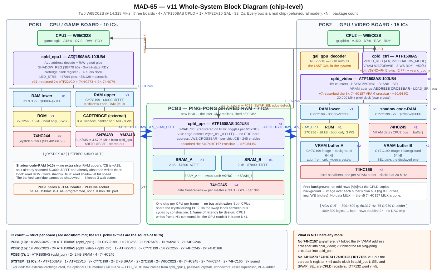
How to read this document. The video engine is three ATF1508AS-10JU84 CPLDs (v7 split; v12 crossbar split-out):
cpld_video(rtl/pcb2/cpld_video.sv, 20 MHz pixel-clock domain) — H/V counters, sync/blank, the VRAM address generator (video_addr), SEL, LOAD_SR,we_copy_nand the pixel path.cpld_ctrl(rtl/pcb2/cpld_ctrl.sv, 14.318 MHz CPU domain) — VIDEO_REG (including SHADOW_MODE, v9), GPU access decode, VRAM/OE//WE//CEsteering, the GPU-data 245 controls, and the 3-wait-state RDY generator for boot-ROM reads (v9; widened to 3 in v10).cpld_xbar(rtl/pcb2/cpld_xbar.sv, v12) — the VRAM address crossbar: muxescpld_video'svideo_addragainst the CPU2 address bus under SEL → both VRAM addresses. Split out ofcpld_videoto give that chip I/O margin (it had reached ~59/60).The crossbar still replaces the old 8× 74HC157 (none were re-added); it just lives on its own CPLD now rather than inside
cpld_video. See §16.4a for the three-chip pin budget and the current inter-chip net list.§2–§12 are organised by function, using the v5 block names ("GAL #1", "6× 74HC163", "74HC374"…). The logic is unchanged — only its housing moved — so the timing, equations and waveforms read identically. Read every such name as the function a CPLD now performs; none of those packages exist on the board. The only discrete video-path chips left are 2× 74HC245 (GPU data) and 2× 74HC166 (pixel serialisers).
One thing left PCB2 entirely and is not in this document's scope: the ping-pong shared RAM (SWAP_SEL, the crossbar, the 4× 245) moved to PCB3's
cpld_pprin v8 — see the architecture doc §6. The VSYNC→IRQ synchroniser went with it in v8 but came back in v14: it lives incpld_ctrlnow, so this board generates VSYNC and the frame/IRQ(§6.1). See §16 for the design history and §13 / §16.5 for the chip count.
| Parameter | Value |
|---|---|
| Logical resolution | 400 × 300 px (1 bit/pixel) |
| Physical resolution | 800 × 600 px (vertical 2× doubling, SVGA fill) |
| Video mode | SVGA 800×600 @ 60.317 Hz (standard) |
| Pixel clock | 20.000 MHz (dedicated crystal) |
| Colour depth | 1-bit: white (1) / black (0) |
| Background copy | hardware, at V[0]=1 (CPLD-sequenced, copy-over-bus) |
| BLANK signal | hardware, generated in the CPLD |
| Hardware scrolling | none |
| BLINDER register | CPLD VIDEO_REG bit 1, written by GPU |
| Background register | CPLD VIDEO_REG bit 0, written by GPU |
| COPY_DIS register | CPLD VIDEO_REG bit 2, written by GPU |
| SHADOW_MODE register (v9) | cpld_ctrl VIDEO_REG bit 3 → decoder GAL; picks $C000–$FFFF overlay (boot: ROM/shadow, run: shadow/VRAM-bg) |
| Boot-ROM wait states | 3 per read (cpld_ctrl RDY generator; v9 added 1, v10 widened to 3) |
| Output standard | VGA/SVGA analogue, 75 Ω |
| Video logic | 3× ATF1508AS-10JU84 CPLD (cpld_video + cpld_ctrl, v7; + cpld_xbar, v12); GPU address decoder folded into cpld_ctrl (v13 — no GAL remains) |
Physical output fills the full SVGA 800×600 frame — 400 logical pixels × 300 logical lines. HSYNC and VSYNC timing is identical to standard SVGA 800×600 @ 60 Hz. All CRT and LCD monitors that accept 800×600 will synchronise correctly with a full-screen image. No black border at top or bottom.
The horizontal and vertical 2× are achieved in completely different ways. This is the key to understanding why the 74HC166 loads every 8 pixel clocks (not every 16) and never needs a shift-enable divider.
Vertical 2× — done by a counter (explicit line repeat).
The V counter runs 0–627 with 600 active lines = 300 logical lines × 2. The VRAM row address
is V[9:1], so V[0] (the low bit) selects the first vs. second physical copy of the same
logical row — each logical line is fetched and displayed twice. There genuinely are 600
distinct scanlines on the wire.
Horizontal 2× — done by the clock rate (free, no counter). A "true" SVGA 800×600 @ 60 Hz dot clock is 40 MHz with 1056 dots/line. This design runs the pixel clock at exactly half that — 20.000 MHz — with 528 H counts/line. Therefore:
1 H count = 1 pixel clock (50 ns) = 1 logical pixel = 2 physical monitor dots
The active window emits 400 distinct pixel values across ~400 clocks; the monitor's analogue raster spreads them over its 800-dot active area, so each value naturally covers two adjacent physical dots. Nothing in the hardware ever holds a bit for two clocks or shifts twice.
Consequence for the shift register. The 74HC166 is clocked at the full 20 MHz and shifts once per logical pixel. It loads a fresh VRAM byte every 8 pixel clocks = 8 logical pixels = 16 physical screen pixels. You would only need "load every 16, shift every 2nd clock" if the pixel clock were the full 40 MHz — because it's 20 MHz, one clock already is one logical pixel and the horizontal ×2 comes for free from the clock rate.
Simulator note. The Verilator/SDL2 sim mirrors this exactly: its framebuffer is 400 columns wide (one entry per H count / per logical pixel), and the SDL2 window stretches it 2× horizontally to 800. So one 74HC166 output bit = one 400-wide framebuffer column = two 800-wide screen columns.
The video circuit datapath is unchanged from v4. SWAP_SEL is no longer here: v5 put it in
GAL #4, v6 folded it into the PCB2 CPLD, and v8 moved it off the board entirely to PCB3's
cpld_ppr. The VSYNC→CPU IRQ synchroniser made the same trip in v8 but returned in v14
(§6.1): cpld_ctrl synchronises VSYNC and drives vsync_cpu_n, and PCB3 recovers the frame edge from
that already-synchronous signal to toggle SWAP_SEL — so the frame IRQ and the ownership swap still
come from one edge detector and stay coherent by construction. See the architecture doc §6.
The VRAM bank-switch SEL flip-flop is a separate thing and does live here — a register
inside cpld_video, toggled on the VSYNC edge (§8). It was a discrete 74HC74 through v5; there
is no 74HC74 on PCB2 now.
H active:         0–399   (400 pixel clocks = 400 logical pixels, each 50 ns)
H front porch:  400–419   (20 clocks,  1.000 µs)
H sync:         420–483   (64 clocks,  3.200 µs, active low)  ← CRT compatible
H back porch:   484–527   (44 clocks,  2.200 µs)
H total:           528 clocks
H frequency:   20 000 000 / 528 = 37 878.8 Hz
V active:         0–599   (600 lines = 300 logical lines × 2)
V front porch:  600–600   (1 line)
V sync:         601–604   (4 lines, active low)  ← same as SVGA 800×600 standard
V back porch:   605–627   (23 lines)
V total:           628 lines
Frame rate:    37 878.8 / 628 = 60.317 Hz
| Signal | Value | Hex | Binary (10-bit H / 10-bit V) |
|---|---|---|---|
| H total | 528 | $210 | 10 0001 0000 |
| H blank start | 400 | $190 | 01 1001 0000 |
| H sync start | 420 | $1A4 | 01 1010 0100 |
| H sync end | 484 | $1E4 | 01 1110 0100 |
| H counter end | 527 | $20F | 10 0000 1111 |
| V total | 628 lines | $274 | 10 0111 0100 |
| V blank start | 600 | $258 | 10 0101 1000 |
| V sync start | 601 | $259 | 10 0101 1001 |
| V sync end | 605 | $25D | 10 0101 1101 |
| V counter end | 627 | $273 | 10 0111 0011 |
Graphical (SVG): MAD65_video_blockdiagram.svg — PCB2
video/VRAM detail; and MAD65_system_blockdiagram.svg for
the whole system. The current (v12) topology — no 74HC157 anywhere; the VRAM address crossbar
is its own CPLD (cpld_xbar), fed by cpld_video's exported video_addr:
20 MHz ─►┌──────────────────────────────────────────────────────────┐
         │  cpld_video   (ATF1508AS-10JU84, pixel-clock domain)      │  ─► HSYNC / VSYNC ─► PCB3
         │   H counter (0–527) · V counter (0–627)                   │  ─► PIXEL_OUT/BG_OUT/BLANK/VIDEO
         │   VRAM addr-gen  addr = V[9:1]·50 + H[9:3]                │  ◄─ qh_a/qh_b (serial pixel)
         │   SEL (double-buffer) · LOAD_SR · we_copy_n               │
         └───┬──────────────────────────────────────────┬───────────┘
   video_addr[13:0] ─► cpld_xbar ◄─ gpu_addr[13:0]      │ load_sr
   cpld_xbar: A/B-addr = SEL ? gpu : video   7 nets ║ (sel, img_oe_n,
             │                                ║   bg_oe_n, we_copy_n,▼
             │                                ▼  cs_*/rdy)     74HC166 ×2 (serialisers)
             │        ┌──────────────────────────────────────┐
             │        │ cpld_ctrl (ATF1508AS, 14.318 domain)  │ ◄─ CPU2 addr/R-W, cs_vram_*
             │        │  VIDEO_REG ($BFE0, 4 bits)            │ ─► rdy (3 wait states)
             │        │  VRAM /CE·/OE·/WE steering            │
             │        │  GPU-data 245 control                 │
             │        └──────────────┬───────────────────────┘
             ▼                       ▼
        VRAM chips A & B        74HC245 ×2 (GPU data ↔ CPU2 bus)
        4× CY7C199
VIDEO_REG ($BFE0) — four bits, latched inside cpld_ctrl (§11):
bit 0: BG_REG — background colour (0=black 0V, 1=dark grey 0.18V)
bit 1: BLINDER — pixel blinder (0=white visible 0.7V, 1=white hidden 0V)
bit 2: COPY_DIS — background copy disable (0=normal copy, 1=VRAM-image frozen)
bit 3: SHADOW_MODE — $C000–$FFFF overlay (v9): 0=boot (read ROM/write shadow), 1=run
VSYNC is generated in cpld_video and drives the SEL double-buffer toggle locally. Since v14
it also crosses one on-board track to cpld_ctrl, whose 2-stage CPU-clock synchroniser produces
vsync_cpu_n (§6.1); that signal drives both CPUs' /IRQ and reaches PCB3, where cpld_ppr
edge-detects it to toggle the registered ping-pong SWAP_SEL. Through v13 the raw VSYNC level
made that trip instead and PCB3 hosted the synchroniser.
The background copy is sequenced by the CPLD over each buffer's own bus (background chip
/OE drives, image chip /WE=WE_COPY latches), so it needs no external data MUX — the v5
74HC157 copy MUX is gone.
CLK ──► [74HC163 #1, bits 0–3] ──RCO──► [74HC163 #2, bits 4–7] ──RCO──► [74HC163 #3, bits 8–11]
        └────────────── LOAD=0 when H=527 (from GAL #1) ─────────────────────────────────────────┘
3× 74HC163 = 12 bits available; 10 bits (H[9:0]) are used (H11, H10 tied to GND or unused). Synchronous reset at H=527: GAL #1 detects H=527 and asserts LOAD with zero on all inputs.
Identical 3× 74HC163 structure. Incremented by V_INC from GAL #1 when H transitions 527→0. Resets to 0 at V=627 and V_INC (i.e. at that line's end), so V holds 627 for a full line and wraps to 0 in step with H_RESET. V_RESET is gated with V_INC inside GAL #2 (v5.0): without the gate the counter would reload 0 one pixel clock after V became 627, holding V=627 for a single clock and starting the next frame at H=1 (blacking the top line's first byte and shortening the frame by ~1 line).
Logical Y address = V[9:1]   (V[0] distinguishes first/second physical line)

74HC166 shift register:
  CLK = CLK_PIX  (full 20 MHz pixel clock — no half-rate trick)
  PE  = LOAD_SR  (active low, from GAL #3)

LOAD_SR fires when H[2:0] == 000 (every 8 pixel clocks):
  → 74HC166 loads new byte from VRAM on next CLK edge
  → each bit is output for exactly 1 pixel clock (50 ns)

NOTE (v5.0): the synchronous load means QH lags the H counter by one CLK_PIX —
byte b's bits appear at H = 8b+1 .. 8b+8, not 8b .. 8b+7.  BLANK_H_RIGHT is
registered by one CLK_PIX in GAL #1 so the active window (H = 1..400) follows the
pixel data: no left-edge stale pixel and no lost right column (399).

Vertical doubling: each logical line displayed twice (V[0]=0 first, V[0]=1 second).
Same byte read at V[0]=0 and V[0]=1 — identical scan line displayed twice.

Bytes per line: H active = 0..399 → H[2:0] cycles 0..7 → 400/8 = 50 loads
50 bytes × 8 bits = 400 logical pixels per line  ✓
Source: rtl/pcb2/cpld_video.sv (pixel-clock domain). These terms were GAL #1 (U_GAL_VIDEO1) through v5; v6 folded them into the CPLD and no such package or reference designator exists on the board — the block name below is a functional grouping only.
H[9:0] — 10 bits of H counter
V0     — bit 0 of V counter (for BG_OE)
HSYNC          — SVGA horizontal sync (active low)
BLANK_H_RIGHT  — H >= 400 (active high)
H_RESET        — H = 527, synchronous load H counter to 0
V_INC          — increment V counter (= H_RESET)
BG_OE          — OE for VRAM-background at V[0]=1 (active low)
BLANK_H_RIGHT = H >= 400:
  H9                    (H = 512..527)
  # H8 & H7 & H6        (H = 448..511)
  # H8 & H7 & H5        (H = 416..447)
  # H8 & H7 & H4        (H = 400..415)

HSYNC active when H = 420..483 (64 clocks, 3.200 µs):
  H8 & H7 & !H6 & H5 & (H4 | H3 | H2)    (H = 420..447)
  # H8 & H7 & H6 & !H5                     (H = 448..479)
  # H8 & H7 & H6 & H5 & !H4 & !H3 & !H2   (H = 480..483)

H_RESET = H = 527:
  H9 & !H8 & !H7 & !H6 & !H5 & !H4 & H3 & H2 & H1 & H0

V_INC = H_RESET

BG_OE = V0
Source: rtl/pcb2/cpld_video.sv (pixel-clock domain). These terms were GAL #2 (U_GAL_VIDEO2) through v5; v6 folded them into the CPLD and no such package or reference designator exists on the board — the block name below is a functional grouping only.
V[9:0] — 10 bits of V counter
VSYNC          — SVGA vertical sync (active low)
BLANK_V_BOTTOM — V >= 600 (active high)
V_RESET        — V = 627, load V counter to 0
V_ACTIVE       — active vertical area (NOT BLANK_V_BOTTOM, to GAL #4)
v14: there is no separate
IRQ_RAWoutput any more. GAL #4 needed one because its synchroniser wanted the active-high level;cpld_ctrltakes the ordinaryvsync_npin and inverts it internally (vsync_s1 <= ~vsync_n), so one signal serves both the VGA connector and the interrupt path. See §6.1.
VSYNC active when V = 601..604 (4 lines — same position as SVGA 800×600 standard):
  V9&!V8&!V7&V6&!V5&V4&V3&!V2&!V1&V0  (V=601)
  # V9&!V8&!V7&V6&!V5&V4&V3&!V2&V1    (V=602, 603)
  # V9&!V8&!V7&V6&!V5&V4&V3&V2&!V1&!V0 (V=604)

BLANK_V_BOTTOM = V >= 600:
  V9 & !V8 & !V7 & V6 & !V5 & V4 & V3    (V = 600..607)
  # V9 & !V8 & !V7 & V6 & V5 & !V4        (V = 608..623)
  # V9 & !V8 & !V7 & V6 & V5 & V4 & !V3 & !V2  (V = 624..627)

V_RESET = V = 627:
  V9 & !V8 & !V7 & V6 & V5 & V4 & !V3 & !V2 & V1 & V0

IRQ_RAW = VSYNC active level (same expression as VSYNC, without negation)

V_ACTIVE = NOT(BLANK_V_BOTTOM) AND NOT(V_RESET)
V = 0–599:   active image (600 physical lines = 300 logical lines × 2)
V = 600:     front porch (1 line)
V = 601–604: VSYNC (4 lines, identical to standard SVGA 800×600 position)
V = 605–627: back porch (23 lines, identical to standard SVGA 800×600)

Result: standard SVGA 800×600 @ 60.317 Hz timing.
Image fills the full active area — no black border.
VSYNC_CPU_N (cpld_ctrl, v14)#Source: rtl/pcb2/cpld_ctrl.sv. This is the system's only clock-domain crossing. VSYNC is
born in cpld_video's 20 MHz clk_pix domain; cpld_ctrl runs on 14.318 MHz clk_14318 (= PHI2),
so it samples vsync_n through two flip-flops and inverts the second:
vsync_s1 <= ~vsync_n        stage 1 — may be metastable
vsync_s2 <= vsync_s1        stage 2 — clean
VSYNC_CPU_N = ~vsync_s2     VSYNC, re-timed to the CPU clock (active low)
VSYNC_CPU_N is a level, low for the whole 4-line VSYNC pulse (~106 µs) — long enough that a
CPU running with interrupts masked still sees it on re-enable. It goes three places: CPU2's /IRQ
on this board, CPU1's /IRQ on PCB1, and PCB3's cpld_ppr, which edge-detects it with a single
flip-flop to toggle SWAP_SEL. One synchroniser, one edge detector, so the frame interrupt and the
ping-pong ownership swap cannot disagree about where a frame begins.
Why the name. Two of the three consumers take it as an interrupt; PCB3 does not — cpld_ppr
only needs the frame boundary. Naming the net irq_n made the shared-RAM board read as if it cared
about interrupts. VSYNC_CPU_N says what the signal is, and the _CPU suffix matches
CLK_CPU/CLK_PIX.
Why stage 2. v8's cpld_ppr tapped stage 1 (irq_out_n = ~irq_s1), which is a one-flip-flop
crossing — a metastable sample could land on both CPUs' /IRQ pins. The second stage costs one
PHI2 (~70 ns) against a 16.6 ms frame.
Why on this board. Through v13 raw VSYNC was cabled to PCB3, synchronised there and the
resulting /IRQ cabled back. PCB2 therefore could not raise its own frame interrupt without PCB3
populated and cabled — an awkward dependency, since VSYNC originates here. Counting flip-flops from
VSYNC, SWAP_SEL still toggles on the same clock edge it did in v8: v8 spent 2 PHI2 reaching its
edge-detect condition and 1 acting on it, v14 spends the first 2 here and the third in cpld_ppr.
Source: rtl/pcb2/cpld_video.sv (pixel-clock domain). These terms were GAL #3 (U_GAL_VIDEO3) through v5; v6 folded them into the CPLD and no such package or reference designator exists on the board — the block name below is a functional grouping only.
H[2:0]          — lower 3 bits of H counter (LOAD_SR detection)
QH              — serial pixel bit from 74HC166
BG_REG          — background colour bit (VIDEO_REG bit 0, from cpld_ctrl)
BLINDER         — pixel blinder bit     (VIDEO_REG bit 1, from cpld_ctrl)
BLANK_H_RIGHT   — from GAL #1 (H >= 400)
BLANK_V_BOT     — from GAL #2 (V >= 600)
LOAD_SR        — load 74HC166 shift register (active low, every 8 clocks)
BLANK          — full BLANK (H and V combined)
PIXEL_OUT      — white pixel in image area (suppressed when BLINDER=1)
BG_OUT         — dark grey background in image area (when BG_REG=1)
VIDEO          — video output (PIXEL_OUT OR BG_OUT)
LOAD_SR = !H2 & !H1 & !H0
  (fires every 8 pixel clocks — byte boundary, H[2:0]=000)

BLANK = BLANK_H_RIGHT # BLANK_V_BOT

PIXEL_OUT = QH & !BLANK & !BLINDER
BG_OUT    = BG_REG & !QH & !BLANK
VIDEO     = PIXEL_OUT # BG_OUT
cpld_ctrl + cpld_video; was GAL #4)#v8 — this section shrank. GAL #4 also held the IRQ synchroniser and SWAP_SEL. Both moved to PCB3's
cpld_ppr(architecture doc §6). SWAP_SEL is still there; the synchroniser came back to PCB2 in v14 and now lives incpld_ctrl— see §6.1, not here. What remains in this section is the VRAM/CEsteering and the background-copy strobe, split across the two CPLDs.
Source: rtl/pcb2/cpld_ctrl.sv (the /CE steering) and rtl/pcb2/cpld_video.sv (we_copy_n).
cpld_ctrl#The front (displayed) buffer is enabled unconditionally; the back (GPU-owned) buffer follows the GPU's own select:
gpu_ce_n   = !( !CS_VRAM_IMG # !CS_VRAM_BG )       ; GPU is touching VRAM at all
a_is_video = !SEL                                  ; A is the front buffer when SEL=0
b_is_video =  SEL

ce_a_n = a_is_video ? 0 : gpu_ce_n
ce_b_n = b_is_video ? 0 : gpu_ce_n
Do not use the old
CS_VRAM_A = (!SEL & VIDEO_EN) # (SEL & GPU_EN)form. That was the v5.1 equation, and it is wrong: it drops the front buffer's/CEon any cycle the GPU takes the bus, blanking the display intermittently. See §16.7. The video side needs the front buffer selected throughout display, which is why the term above is a constant 0.
The per-chip /OE and /WE are steered the same way — the front buffer's image chip takes
img_oe_n/we_copy_n from cpld_video, the back buffer's takes the GPU's.
v16 — the GPU side of that mux is PHI2-qualified, the video side is not. The GPU write terms carry the gate at their source:
GPU_WE_IMG = !CS_VRAM_IMG & !R/W & PHI2
GPU_WE_BG  = !CS_VRAM_BG  & !R/W & PHI2
so a VRAM write commits on PHI2's falling edge with address and data still valid — the same rule every other write sink in the system now follows (address-decoder doc §3a).
WE_COPYis deliberately exempt: it is generated bycpld_videoin the 20 MHzclk_pixdomain for the background→image copy and has nothing to do with the CPU bus, so gating it with PHI2 would be meaningless and would break the copy.
cpld_video#WE_COPY = !( !BG_OE & V_ACTIVE & CS_VRAM_IMG & !COPY_DIS & !BLANK_HR )
!BG_OE — the background chip is driving (odd rows, V[0]=1)V_ACTIVE — vertical active areaCS_VRAM_IMG — the GPU is not accessing the image chip (active-low select, so high = idle)!COPY_DIS — copy enabled (VIDEO_REG bit 2 clear)!BLANK_HR — the horizontal active region only. Essential: copy_win keys only on
h[2:0], so without this gate the strobe keeps firing past H=400 during blanking and
corrupts VRAM beyond the visible line. Added in v6 — see §16.7.cpld_video#SEL is a register inside cpld_video, toggled on the VSYNC edge:
SEL=0: Video reads VRAM_A, GPU writes VRAM_B
SEL=1: Video reads VRAM_B, GPU writes VRAM_A
SEL also steers the VRAM address crossbar, which lives in its own CPLD cpld_xbar since
v12 (it was folded into cpld_video in v7, and 8× 74HC157 through v6). SEL is exported from
cpld_video to both cpld_ctrl and cpld_xbar (§16.4a).
There is no external 74HC74 — the SEL flip-flop moved into the CPLD in v6, and the ping-pong
SWAP_SEL that once shared that package is now a register in cpld_ppr on PCB3, clocked by PHI2.
vram_addr = V[9:1] × 50 + H[9:3]
Where:
- V[9:1] = logical line 0–299
- H[9:3] = byte in line 0–49
Verification: - H active = 0..399 → H[9:3] = 0..49 (50 bytes/line) ✓ - 74HC166 loaded every 8 pixel clocks: H[9:3] stable during each load cycle ✓ - max addr = 299 × 50 + 49 = 14,999 = $3A97 (14 bits, well within 32 kB chip) ✓ - GPU window ($8000–$BFDF = 16,352 bytes): max GPU addr = $8000+$3A97 = $BA97 < $BFDF ✓
50 = 32 + 16 + 2 = 2⁵ + 2⁴ + 2¹

Y = V[9:1]  (9 bits, value 0–299)
Y × 32 = {Y, 0, 0, 0, 0, 0}   ← bit shift, zero gates
Y × 16 = {Y, 0, 0, 0, 0}      ← bit shift, zero gates
Y × 2  = {Y, 0}                ← bit shift, zero gates

Stage 1: Y×32 + Y×16 = Y×48   ← 3× 74HC283 (14-bit addition)
Stage 2: Y×48 + Y×2  = Y×50   ← 1× 74HC283 (Y×2 adds into bits [8:1])
Stage 3: Y×50 + H[9:3]        ← 1× 74HC283 (final byte-address addition)
Total: 5× 74HC283 adders.
The image and background chips of a buffer share one bidirectional data bus. A single-
port SRAM cannot output and be written at the same instant, so image read (for display) and
background copy (write) are sequenced within the 8-clock byte window. Define the
copy window = H[2:0] ∈ {4,5} (H2 & !H1). IMG_OE and BG_OE (both GAL #1) are exact
complements, so exactly one chip drives the bus at any time — the 74HC157 copy MUX is gone.
H[2:0]:   0    1    2    3    4    5    6    7
IMG_OE   ██████████████       ·    ·   ██████   image chip /OE (drives bus)
 LOAD_SR ▲ 74HC166 loads image byte off the bus (GAL #3)
BG_OE     ·    ·    ·    ·   ██████    ·    ·    background chip /OE  (V[0]=1 only)
WE_COPY   ·    ·    ·    ·   ██████    ·    ·    image chip /WE       (V[0]=1 only)

V[0]=0 (first physical line):  copy window idle (BG_OE/WE_COPY need V[0]=1) — image
       drives the whole window; byte displayed, VRAM untouched.
V[0]=1 (second physical line): image drives + loads the 166 (display, identical to V[0]=0);
       then in {4,5} the background chip drives the bus and the image chip's /WE latches it
       — the "free background" copy, over the shared bus. Inhibited when COPY_DIS=1.
The Verilator model is structural: rtl/mem/sram_io.sv is the CY7C199 with a real
tri-state inout dq, and the VRAM interconnect (4× SRAM, 2× 245, 2× 166) is inlined directly
into rtl/pcb2/pcb2.sv. cpld_ctrl puts the image+background chips of each buffer on one
shared bus and sequences /OE,/WE by ownership and phase.
The video-owned buffer stays /CE-enabled throughout scanout — ce_a_n = a_is_video ? 0 :
gpu_ce_n (§8). This is not an optimisation: the older (!SEL & VIDEO_EN) form dropped the front
buffer's /CE on any cycle the GPU took the bus, which blanked the display intermittently. The
GPU-owned buffer uses gpu_ce_n.
An earlier revision of this section said the 74HC245 bus-buffer layer was "not yet modelled" and that the module lived in
rtl/pcb2/video/vram_sys.sv. Both are obsolete: the 245s are modelled (pcb2.sv—u_245_a/u_245_b), andvram_sys.svand the wholertl/pcb2/video/directory were removed when the interconnect was inlined. See §16.7–§16.8.
H=0:  H[2:0]=0, LOAD_SR asserted (load happens on the H=0→1 edge)
H=1:  QH=b7   (byte b's first pixel; active because BLANK_H_RIGHT is delayed 1 clk)
H=2:  QH=b6
H=3:  QH=b5
H=4:  QH=b4
H=5:  QH=b3
H=6:  QH=b2
H=7:  QH=b1
H=8:  QH=b0 ; H[2:0]=0 again → next LOAD_SR (next byte's b7 appears at H=9)

So byte b occupies H = 8b+1 .. 8b+8.  The active window is H = 1..400 (BLANK_H_RIGHT
registered one CLK_PIX), so all 400 columns (byte 0 col 0 .. byte 49 col 7) display
and column 399 is not blanked.

(V[0]=1 only, copy window H[2:0] ∈ {4,5}):
  BG_OE → background chip drives the shared data bus (A14=1, same address generator)
  WE_COPY (GAL #4, combinatorial) → image chip /WE latches the background byte
  Outside the copy window IMG_OE re-enables the image chip (single bus driver at all times)
bit 0:   BG_REG   — background colour register
           0 → black background pixels    (0.00 V)
           1 → dark grey background pixels (0.18 V)
           → to GAL #3

bit 1:   BLINDER  — pixel blinder register
           0 → white (bitmap=1) pixels visible   (0.70 V)  — normal
           1 → white (bitmap=1) pixels suppressed (0.00 V) — bitmap hidden
           → to GAL #3

bit 2:   COPY_DIS — background copy disable register
           0 → normal: VRAM-background copied to VRAM-image at each V[0]=1 line
           1 → frozen: WE_COPY inhibited, VRAM-image NOT modified by video circuit
           → to cpld_video's we_copy_n term

bit 3:   SHADOW_MODE — GPU code-RAM overlay select (v9)   → to decoder GAL
           0 → boot: read $C000–$FFFF from ROM (+3 wait states), write to shadow code-RAM
           1 → run:  read $C000–$FFFF from shadow code-RAM (full speed), write to VRAM-background
           reset value 0 (reset vector fetches from ROM); set once at boot, kept set

bits 7–4: reserved (not used)
SHADOW_MODE / shadow code-RAM (v9): cpld_ctrl holds VIDEO_REG bit 3 as shadow_mode
(an internal wire since v13 folded the decoder in — was fed off-chip to gal_gpu_decoder), and
uses it to steer $C000–$FFFF three ways — /CS_ROM, /CS_SHADOW, /CS_VRAM_BG.
cpld_ctrl also holds rdy (RDY) low for three PHI2 cycles on each ROM read, so a boot-ROM
access spans 4 cycles (~239 ns of access time — ample for any EPROM grade). A 2-bit counter
re-arms at 3, giving every back-to-back fetch its own fresh 3 wait states:
rdy = !( ROM_ACCESS & (WCNT != 3) ) ; cpld_ctrl.sv
This costs nothing at run time: /CS_ROM is SHADOW_MODE-gated, so the ROM is only read during
the boot copy. v9 introduced one wait state; v10 widened it to three. See
MAD65_architecture.md §5.
BLINDER / BG_REG — output levels in active image area:
| BLINDER | BG_REG | bitmap=1 pixel | bitmap=0 pixel |
|---|---|---|---|
| 0 | 0 | 0.70 V (white) | 0.00 V (black) |
| 0 | 1 | 0.70 V (white) | 0.18 V (grey) |
| 1 | 0 | 0.00 V (black) | 0.00 V (black) |
| 1 | 1 | 0.00 V (black) | 0.18 V (grey) |
COPY_DIS — background copy mechanism:
| COPY_DIS | Effect on VRAM-image each V[0]=1 line |
|---|---|
| 0 | Normal: VRAM-background byte written to VRAM-image (WE_COPY) |
| 1 | Frozen: WE_COPY inhibited — VRAM-image content preserved |
BLANK area (outside active image): always 0.00 V — VGA/SVGA compliant.
Pin 1  ── RED   ── PIXEL_OUT (75Ω) + BG_OUT (270Ω) ──┐
Pin 2  ── GREEN ── PIXEL_OUT (75Ω) + BG_OUT (270Ω) ──┤ (tied → monochrome)
Pin 3  ── BLUE  ── PIXEL_OUT (75Ω) + BG_OUT (270Ω) ──┘
Pin 5  ── GND
Pin 6  ── RED_RTN  ── GND
Pin 7  ── GRN_RTN  ── GND
Pin 8  ── BLU_RTN  ── GND
Pin 13 ── HSYNC ── from the CPLD (hsync_n output)
Pin 14 ── VSYNC ── from the CPLD (vsync_n output)
PIXEL_OUT=1, BLINDER=0, BLANK=0  → 75Ω  → ~0.70 V  (white)
BG_OUT=1,    BG_REG=1,  BLANK=0  → 270Ω → ~0.18 V  (dark grey)
Both=0                            →        0.00 V   (black)
BLANK=1                           →        0.00 V   (blanking — SVGA compliant)
The v7 video module (PCB2), as modelled in rtl/pcb2/pcb2.sv / cpld_video.sv / cpld_ctrl.sv:
| Component | Function | Qty |
|---|---|---|
| ATF1508AS-10JU84 | CPLD cpld_video — H/V counters, sync/blank, VRAM addr-gen (video_addr), SEL, LOAD_SR, pixel path (≈33/64 I/O since v12) |
1 |
| ATF1508AS-10JU84 | CPLD cpld_ctrl — the GPU address decoder (v13, was the ATF22V10 gal_gpu_decoder), VIDEO_REG (incl. SHADOW_MODE, v9), GPU decode, VRAM /OE//WE//CE steering, 245 control, 3-wait-state RDY generator (v9/v10), the VSYNC→PHI2 synchroniser → vsync_cpu_n (v14, §6.1) LED_STRB (v15) and the PHI2-qualified /WE (v16) (≈52/64 I/O). SWAP_SEL left for PCB3's cpld_ppr in v8 and stayed there |
1 |
| ATF1508AS-10JU84 | CPLD cpld_xbar (v12) — the VRAM address crossbar: A/B-addr = SEL ? gpu_addr : video_addr (≈57/64 I/O). Split out of cpld_video for I/O margin |
1 |
| 74HC245 | GPU data transceivers (CPU2 bus ↔ back buffer) | 2 |
| 74HC166 | Pixel serialisers (one per buffer; cpld_video picks by SEL) |
2 |
| 74HC574 | v15: LED_GPU_REG ($BFC0–$BFDF) — 8 diagnostic LEDs, clocked by LED_STRB from cpld_ctrl. Not part of the video path |
1 |
| CY7C199-15PC | VRAM — image A/B + background A/B | 4 |
| Resistor 75 Ω | VGA white output (R, G, B) | 3 |
| Resistor 270 Ω | VGA dark grey background output (R, G, B) | 3 |
| Crystal 20.000 MHz | SVGA pixel clock (standard 800×600 @ 60 Hz) | 1 |
Video logic + interconnect: 3 CPLD (v12) + 4 discrete (2× 245 + 2× 166). The ~16-chip v5 discrete
video pile (4× ATF22V10 video GAL, 6× 74HC163, 5× 74HC283, 74HC374, 74HC74 SEL) collapsed into one
CPLD in v6; v7 adds a second CPLD to absorb the 8× 74HC157 VRAM address crossbar as well, so
only the data transceivers and serialisers remain discrete. The GPU decoder folded into
cpld_ctrl in v13 (the last ATF22V10 — no GAL remains). Note the ping-pong shared-RAM
interconnect is a separate subsystem — on its own board PCB3 as of v8 (2× SRAM + 4× 74HC245 +
cpld_ppr, which absorbs the former 6× 74HC157 crossbar) — see the architecture doc §6.
| Feature | v1 (TTL only) | v2 (2 GAL) | v3 (4 GAL) | v4 | v5 |
|---|---|---|---|---|---|
| Total ICs | 18–22 | 16–17 | 17 + ext. comparator | 17 | 17 (SWAP_SEL in GAL #4) |
| BLANK signal | none | yes | yes (all 4 edges) | yes (H+V, no scroll) | yes (unchanged) |
| BG_REG register | none | yes | yes | yes (74HC374 bit 0) | yes (unchanged) |
| BLINDER register | none | none | none | yes (74HC374 bit 1) | yes (unchanged) |
| COPY_DIS register | none | none | none | yes (74HC374 bit 2) | yes (unchanged) |
| Shared RAM swap | — | — | — | IDT7132 (dual-port) | ping-pong, sync swap (GAL #4) |
| Background copy mechanism | none | none | yes (74HC157 MUX) | yes + COPY_DIS inhibit | yes (unchanged) |
| Logical resolution | — | — | 384×240 (incorrect) | 400×300 | 400×300 (unchanged) |
| Physical resolution | — | — | 768×480 (non-standard) | 800×600 (full SVGA) | 800×600 (unchanged) |
| Pixel clock | 25.175 MHz | 25.175 MHz | 25.175 MHz | 20.000 MHz | 20.000 MHz (unchanged) |
| Ver | Change to the video module |
|---|---|
| v6 | All v5 video logic — the four GALs, 6× 74HC163, 5× 74HC283, the 74HC374 VIDEO_REG and the 74HC74 SEL FF — folded into one ATF1508AS CPLD (cpld_pcb2). Behaviour unchanged; only the housing moved. The VRAM data path became structural (8× 74HC157 + 2× 74HC245 + 2× 74HC166). |
| v7 | cpld_pcb2 split into cpld_video + cpld_ctrl — the second chip made room to absorb the 8× 74HC157 VRAM address crossbar, which disappeared. §16.4a. |
| v8 | The ping-pong shared RAM left PCB2 for its own board, PCB3. cpld_ctrl shed SWAP_SEL, the VSYNC→IRQ synchroniser and the ping-pong 245 enables to cpld_ppr, which also absorbed the 6× 74HC157 ping-pong crossbar. gal_gpu_decoder now emits a single cs_sram_gpu_n. PCB2: 26 → 14 ICs. |
| v9 | Shadow code-RAM (u_shadow, a 6th CY7C199) at $C000–$FFFF so GPU code runs from fast SRAM. VIDEO_REG gains bit 3 = SHADOW_MODE; cpld_ctrl gains a wait-state RDY generator; the decoder GAL gains shadow_mode in / cs_shadow_n out. PCB2: 15 ICs. |
| v10 | Boot-ROM wait states widened 1 → 3 (~239 ns of access time). Free — the ROM is only read during the boot copy. |
| v11 | PCB1-only (its two GALs → cpld_cpu1). No change to the video module; system total 36 → 32 ICs. |
| v12 | The VRAM address crossbar split out of cpld_video into its own ATF1508AS (cpld_xbar), freeing cpld_video from ~59/60 to ~33/64 usable I/O. cpld_video now exports video_addr[13:0]; cpld_xbar muxes it against the CPU2 bus under SEL. No discrete 74HC157 returned. PCB2: 15 → 16 ICs; system total 32 → 33 ICs. §16.4a. |
| v13 | The GPU address decoder — the last ATF22V10 (gal_gpu_decoder) — folded into cpld_ctrl (~37 → ~48/64 I/O). The CPU2 address bus a15..a5 now enters that chip and shadow_mode stops round-tripping off-chip. No GAL remains anywhere in MAD-65. PCB2: 16 → 15 ICs. |
| v14 | The VSYNC→PHI2 synchroniser came back to PCB2, into cpld_ctrl (~48 → ~50/64 I/O): cpld_video's vsync_n crosses one on-board track, two flip-flops guard metastability, and vsync_cpu_n (off stage 2, not stage 1 as v8 had it) drives CPU2 locally and leaves the connector for PCB1 and PCB3. PCB3 keeps SWAP_SEL but only edge-detects the now-synchronous vsync_cpu_n — one flip-flop, no CDC — and cpld_ppr drops 60 → 59/64 I/O. Raw VSYNC no longer leaves PCB2 except to the VGA connector, so the video module raises its own frame interrupt standalone. No IC-count change. |
| v15 | LED_STRB added to cpld_ctrl (~50 → ~51/64 I/O) and the GPU diagnostic LED register populated on-board: one 74HC574 at $BFC0–$BFDF, write-only, clocked by the rising edge of LED_STRB (active-high, PHI1-gated). Not a video-path change — it is here because cpld_ctrl owns the GPU decode. The 74HC133 the original design specified is retired unbuilt (it only ever existed because the pre-v13 ATF22V10 had no spare macrocell). gpu_os has written LED_GPU_REG since it was written — four boot POST stages plus the GPU_LED opcode — and until now nothing latched it. PCB2: 15 → 16 ICs; system total 32 → 33 ICs. |
| v16 | All write strobes PHI2-qualified: /WE = ~(PHI2 & ~R/W), emitted by each board CPLD (cpld_ctrl ≈51 → ≈52/64 I/O). Through v15 every /WE in the system was raw R/W — a real defect, since an async SRAM commits on /WE's rising edge and that edge landed after the CPU had released the write data, with back-to-back pushes never releasing /WE at all. On PCB2 the gate also folds into gpu_we_img / gpu_we_bg, so all four VRAM chips get it. we_copy_n is exempt — it is a clk_pix-domain video strobe, not a CPU write. No IC-count change. See the address-decoder doc §3a. |
Current: v16. The video module is 3× ATF1508AS + 2× 74HC245 + 2× 74HC166, plus 4× CY7C199 VRAM. No 74HC157, 74HC163, 74HC283, 74HC374 or 74HC74 remains — see §13 and §16. (v15's 74HC574 is the LED latch, outside the video path.)
WE_COPY timing — BG_OE is combinatorial (V0). WE_COPY fires after one cpld_video
propagation delay (≤10 ns for a -10 part). At 20 MHz one clock = 50 ns.
CY7C199: tAW ≥ 0 ns, tDW ≥ 25 ns — ample margin. Verify on prototype.
74HC166 CLK = CLK_PIX — 74HC166 clocked at full 20 MHz. Setup time ~5 ns, hold time ~5 ns. At 20 MHz (50 ns clock): 45 ns margin. ✓
Bus conflict during WE_COPY — during WE_COPY the VRAM-image data bus is driven by the
VRAM-background chip over the buffer's own bus (there is no MUX; the v5 74HC157 copy MUX
was removed in v5.1 — §10). The GPU's 74HC245 must be off for that buffer, which
cpld_ctrl's oe245_a/b_n guarantee: they only enable on ~gpu_ce_n, and we_copy_n is
itself gated by cs_vram_img_n (GPU not touching the image chip). §8.
VSYNC to IRQ delay — ~~(GAL #4 FF)~~ Back on this board since v14. cpld_ctrl runs
VSYNC through a 2-stage synchroniser to CLK_14318 (2 clocks ≈ 140 ns) and drives
vsync_cpu_n; PCB3's cpld_ppr derives SWAP_SEL from that same signal one clock later, so the
frame IRQ and the ownership swap stay coherent. Acceptable for a 60 Hz IRQ. See §6.1 and the
architecture doc §6. (v8–v13: a 3-stage synchroniser on PCB3, ≈210 ns, with /IRQ off stage 1.)
COPY_DIS usage pattern — set/clear during VBLANK to avoid mid-line artefacts. When COPY_DIS=1, background data in VRAM-background is preserved unchanged.
VRAM-background A14 hardwired — background chip A14 must be tied to VCC (via 100 Ω) from the video address bus side. Background data stored at chip offset $4000 (GPU writes $C000 → chip A14:0=$4000). Video address generator A13:0 connects to both image chip and background chip; A14=1 on background chip only.
GAL #4 SWAP_SEL budget — ~~(SWAP_SEL + IRQ_S2/IRQ_S3 → 8/10 macrocells; verify the fit
when re-compiling GAL #4)~~ Obsolete — there is no GAL #4. v6 folded it into the CPLD and
v8 moved SWAP_SEL and the sync stages off PCB2 to cpld_ppr on PCB3 (≈60/64 I/O — see the
architecture doc §16 open issue 10 for the live CPLD I/O budgets). Nothing to verify.
⚠️ This section is HISTORY, not the current design. It documents the v6 consolidation that collapsed the discrete logic-glue pile into a single CPLD (
cpld_pcb2.sv) — a file and a partition that no longer exist. Two later revisions superseded its conclusions:
- v7 split that one chip into
cpld_video+cpld_ctrl, which absorbed the 8× 74HC157 VRAM address crossbar. §16.4a below is the current, authoritative partition — read it rather than §16.4.- v8 moved the whole ping-pong subsystem (SWAP_SEL, the IRQ synchroniser, the 6× 74HC157 crossbar, the 4× 245, the 2× SRAM) off PCB2 onto PCB3. Every mention of ping-pong parts "on PCB2" below is v6-era — see the architecture doc §6 for the real thing.
It is kept because the reasoning (why consolidate, what the budget looked like, which bugs it fixed) is still useful. For what is actually on the board today, see the masthead, §8 and §13. §§1–15 above specify the video logic itself.
Two problems drove this:
rtl/pcb2/video/vram_sys.sv faked the crossbar
with behavioral ? : muxes (e.g. a_addr = a_is_video ? video_addr : gpu_addr). Those
are not models of any real chip, so they can never validate hardware.The fix for both: put the address muxes and data buffers back as real 74xx parts, and
sweep the rest of the video logic — all four video GALs, the H/V counters, the VRAM address
generator, the video register, and every steering/arbitration term — into a single
ATF1508AS-10JU84 CPLD (128 macrocells, 64 I/O, synthesizable SystemVerilog). The address
decoder stays a separate ATF22V10 GAL (see §16.2): it is a stable combinational
address→chip-select map that has no need of the video timing, and keeping it out of the CPLD
frees ~8 input pins (the CPU A15:A5 bus never enters the CPLD). (This held through v12; v13
folded the decoder into cpld_ctrl after all — that chip had the spare I/O — retiring the last
ATF22V10. The A15:A5 bus now enters cpld_ctrl. See §16.4a.)
This aligns perfectly with the project's modelling rule: real chips get behavioral models;
everything else is structural wiring. The CPLD is a real chip, so its behavioral model is
legitimate. The ? : glue is not re-modeled — it is partitioned: address muxes become
74HC157 instances, data buffers become 74HC245/74HC166 instances, and the arbitration
logic moves inside the CPLD behavioral model.
| Function (v5.1) | v5.1 parts | v6 home |
|---|---|---|
Address decoder (gpu_decoder GAL) |
1× ATF22V10 | separate GAL (unchanged) |
| Video GAL #1–#4 (sync, blank, CS, WE_COPY, IRQ sync, SWAP_SEL) | 4× ATF22V10 | CPLD |
| H counter + V counter | 6× 74HC163 | CPLD |
| VRAM address generator (V·50 + H) | 5× 74HC283 | CPLD |
| VIDEO_REG (BG_REG / BLINDER / COPY_DIS) | 1× 74HC374 | CPLD |
| VRAM-SEL / SWAP_SEL / IRQ sync flip-flops | 1× 74HC74 | CPLD |
All control steering (the vram_sys ? : glue) |
(faked in sim) | CPLD |
| Address crossbar (video_addr vs gpu_addr → each buffer) | (faked) | 8× 74HC157 |
| GPU VRAM data buffers (CPU2 bus ↔ back buffer, bidir) | (faked) | 2× 74HC245 |
| Video-read serialisers (front buffer → pixel) | 1× 74HC166 | 2× 74HC166 |
| VRAM chips | 4× CY7C199 | unchanged |
| CPU2 / RAM / ROM / ping-pong SRAM | unchanged | unchanged |
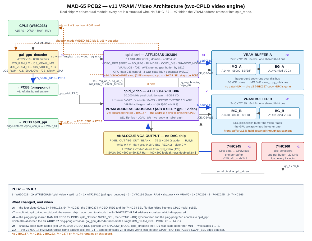
(ASCII version of the same diagram below, for terminals / diff review.)
  CPU2 A15:A5, R/W ─►┌────────────────────┐─► cs_rom_n, cs_ram_lo_n, ce_sram_a/b_n → chips
  cpu1_ce/we ───────►│  ATF22V10 DECODER  │─► cs_vram_img_n, cs_vram_bg_n, cs_video_reg_n ──┐
  swap_sel ─────────►│ (gal_gpu_decoder,  │      (decoded VRAM/reg selects → CPLD)          │
       │             │  unchanged v5.1)   │                                                 │
       │             └────────────────────┘                                                 │
       │   clk_pix, clk_14318, rst_n ─┐   D2:D0, R/W ─┐   qh_a, qh_b ◄─(from 166s below)     │
       │                              ▼               ▼          ▼                          ▼
       │    ┌──────────────────────────────────────────────────────────────────────────────┐
       └────┤ swap_sel           ATF1508AS-10JU84  (CPLD)                                    │
            │  GAL#1–4 · H/V counters · addr-gen (V·50+H) · VIDEO_REG                        │
            │  · SEL/SWAP/IRQ FFs · ALL control steering                                     │
            └──────────────────────────────────────────────────────────────────────────────┘
   video_addr[13:0]│ SEL│ VRAM /CE·/OE·/WE ×10│ 245 ctl│ load_sr │ hsync/vsync/pixel/bg/blank
                   ▼    ▼                     ▼   (to both 166s)
   gpu_addr[13:0] ─►┌───────────────────────┐
   (CPU2 A13:0)     │   8× 74HC157           │  A-addr = SEL ? gpu   : video
                    │   ADDRESS CROSSBAR     │  B-addr = SEL ? video : gpu
                    └───┬───────────────┬────┘
                  A13:0 │         A13:0 │
              ┌─────────┴───┐   ┌───────┴─────┐
              │ IMG_A  BG_A │   │ IMG_B  BG_B │   4× CY7C199
              │  bus data_a │   │  bus data_b │   (A14=0 image, A14=1 background)
              └──┬───────┬──┘   └──┬───────┬──┘
          data_a│       │data_a    │data_b │data_b
                ▼       │          ▼       │
           74HC166_A    │     74HC166_B    │     both always load @ LOAD_SR;
                │qh_a───┘          │qh_b───┘     CPLD selects qh_a/qh_b by SEL
                │                  │             (1-bit serial mux — free)
             ┌──┴───┐           ┌──┴───┐
             │74HC245│ CPU2 D ◄──┤74HC245│  GPU R/W to the BACK buffer; the one
             └──────┘   bus      └──────┘  whose buffer is GPU-owned is enabled,
                                           dir = R/W (write CPU2→bus, read bus→CPU2)
Why dual 74HC166 (vs. one 166 + an 8-bit data mux): with two serialisers the CPLD only
needs the two 1-bit outputs qh_a/qh_b and picks one by SEL internally — a free 2:1 in
the fabric. The wide data_a/data_b buses therefore never enter the CPLD, which is
what keeps the I/O budget inside 64 pins. Both 166s load every byte off their own buffer's
bus; only the front-buffer serialiser's output is used.
Copy-over-bus is unchanged and stays internal to each buffer: during the copy window the
background chip's /OE drives its buffer bus while the image chip's /WE (WE_COPY) latches
it — image and background of a buffer still share one bus (§10), so the copy needs no external
buffering. The CPLD sequences /OE///WE exactly as GAL #1/#4 did in v5.
v7/v12 note. The video engine is now three ATF1508AS (
cpld_video+cpld_ctrl+cpld_xbar). The single-chip v6 budget (≈ 55/64 below, historical) could not also absorb the VRAM address crossbar: internalising it costs +28 pins (two 14-bit VRAM addresses out, +14 for the CPU2 address in, −14 for thevideo_addrit replaces). v7 put the crossbar incpld_video, which drove that chip to ≈ 59/60 — no fitting margin — so v12 moved the crossbar to its own chipcpld_xbar(no discrete 74HC157 re-added). See §16.4a for the current three-chip budget.
Decoder external, so the CPU address bus does not reach cpld_ctrl; it takes only the
decoded selects it consumes.
v6 single-chip budget (historical):
| Dir | Signals | Pins |
|---|---|---|
| In | clk_pix (20 MHz), clk_14318, rst_n |
3 |
| In | cs_vram_img_n, cs_vram_bg_n, cs_video_reg_n, R/W (from decoder GAL) |
4 |
| In | D2:D0 (VIDEO_REG), qh_a, qh_b |
5 |
| In | cpu1_ce_sram_n, ce_sram_a_n, ce_sram_b_n (ping-pong 245 enable terms) |
3 |
| Out | video_addr[13:0] (→ address crossbar) |
14 |
| Out | SEL (crossbar select + qh serial mux), load_sr_n, irq_out, swap_sel (→ decoder) |
4 |
| Out | VRAM control: {ce, img_oe, img_we, bg_oe, bg_we} × buffer A/B |
10 |
| Out | GPU 245 control: /OE_a, /OE_b, DIR |
3 |
| Out | Ping-pong 245 control: oe_cpu1_a, oe_cpu1_b, oe_gpu_a, oe_gpu_b |
4 |
| Out | hsync_n, vsync_n, pixel_out, bg_out, blank |
5 |
| Total | ≈ 55 / 64 |
This subsection is the authoritative partition, unlike §16.4 above it. Ports match
rtl/pcb2/cpld_video.sv,rtl/pcb2/cpld_ctrl.svandrtl/pcb2/cpld_xbar.sv.
CPLD #1 cpld_video (20 MHz pixel-clock domain) — counters, sync/blank, VRAM
address-gen (video_addr), SEL, LOAD_SR, we_copy_n, pixel path. v12 lifted the VRAM
address crossbar out to cpld_xbar (CPLD #3), so this chip no longer takes the CPU2 address
bus or drives the VRAM addresses; it exports its internal video_addr instead:
| Dir | Signals | Pins |
|---|---|---|
| In | clk_pix, rst_n, qh_a, qh_b, cs_vram_img_n, bg_reg, blinder, copy_dis |
8 |
| Out | video_addr[13:0] (→ cpld_xbar) |
14 |
| Out | hsync_n, vsync_n, blank, pixel_out, bg_out, load_sr_n |
6 |
| Out | sel, img_oe_n, bg_oe_n, we_copy_n (→ cpld_ctrl; sel also → cpld_xbar) |
4 |
| Total | ≈ 33 / 64 |
vsync_n is a board output and, since v14, also an on-board net to cpld_ctrl's
synchroniser (§6.1) — one pin, two loads, no extra I/O on this chip. It no longer goes to PCB3.
sel is a real pin (it feeds cpld_ctrl and cpld_xbar) but it stays on PCB2 — it is not a
port of pcb2 or mad65_top. The SDL harness reads the flip-flop itself, sel_r, which carries
/*verilator public_flat_rd*/, exactly as it reads the h[9:0]/v[9:0] counters — those are
Verilator/SDL introspection taps only, not physical pins and not module ports either.
CPLD #2 cpld_ctrl (14.318 MHz domain) — the GPU address decoder (v13, folded in from
gal_gpu_decoder), VIDEO_REG (incl. SHADOW_MODE), VRAM /OE//WE//CE steering, GPU-data 245
control, the 3-wait-state RDY generator:
| Dir | Signals | Pins |
|---|---|---|
| In | clk_14318, rst_n, a15..a5 (CPU2 address, v13 — 11), gpu_rw, gpu_din[7:0], sel, img_oe_n, bg_oe_n, we_copy_n |
26 |
| In | vsync_n (← cpld_video, v14 — the CDC input, §6.1) |
1 |
| Out | decode selects cs_ram_lo_n, cs_sram_gpu_n (→PCB3), cs_rom_n, cs_shadow_n, cs_vram_img_n (→cpld_video) — v13 |
5 |
| Out | VRAM control {ce, img_oe, img_we, bg_oe, bg_we} × A/B |
10 |
| Out | GPU 245 oe245_a_n, oe245_b_n, dir245 |
3 |
| Out | bg_reg, blinder, copy_dis (→ cpld_video), rdy (v9/v10 → CPU2) |
4 |
| Out | vsync_cpu_n (v14 → CPU2 locally, PCB1, PCB3) |
1 |
| Total | ≈ 50 / 64 |
v14:
vsync_nreturns as an input andvsync_cpu_nappears as an output — the VSYNC→PHI2 synchroniser (§6.1). Net +2 pins (48 → 50). PCB3'scpld_pprloses itsvsync_ninput andirq_out_noutput in exchange for onevsync_cpu_ninput (60 → 59).v13:
cs_vram_bg_n,cs_video_reg_nandshadow_modeare now internal to this chip (they only ever fedcpld_ctrlor the decoder);cs_rom_nandcs_vram_img_nflipped from inputs to outputs. Net +11 pins (37 → 48), retiring the last ATF22V10.v14:
vsync_nreturns as an input andvsync_cpu_nappears as an output — the VSYNC→PHI2 synchroniser and the frame interrupt (§6.1). Net +2 pins (48 → 50). PCB3'scpld_pprloses itsvsync_ninput andirq_out_noutput in exchange for onevsync_cpu_ninput (60 → 59).What v8 and v9 changed here. v8 removed the ping-pong control from
cpld_ctrlentirely —cpu1_ce_sram_n,ce_sram_a/b_n,vsync_n,swap_sel,irq_outand the four ping-pong 245 enables all went to PCB3'scpld_ppr. (vsync_ncame back in v14 — see above — but for the IRQ synchroniser only; SWAP_SEL stayed on PCB3.) v9 added the shadow code-RAM signals: incs_rom_n, outshadow_mode+rdy; the decoder GAL correspondingly gained ashadow_modeinput and acs_shadow_noutput (architecture doc §5). v10 widened the wait states 1 → 3 (no pin change).
CPLD #3 cpld_xbar (v12) — the VRAM address crossbar, on its own chip. Purely
combinational (no clock/reset): it muxes cpld_video's video_addr against the CPU2 address
bus under SEL and drives both VRAM buffer addresses. Equations are verbatim the old
cpld_video crossbar (a_addr = sel ? gpu_addr : video_addr, b_addr the swap):
| Dir | Signals | Pins |
|---|---|---|
| In | gpu_addr[13:0] (CPU2 A13:0), video_addr[13:0] (← cpld_video), sel (← cpld_video) |
29 |
| Out | a_addr[13:0], b_addr[13:0] (→ VRAM chips) |
28 |
| Total | ≈ 57 / 64 |
Inter-chip nets = 22: cpld_video → cpld_ctrl = sel, img_oe_n, bg_oe_n, we_copy_n;
cpld_ctrl → cpld_video = bg_reg, blinder, copy_dis (VIDEO_REG bits — quasi-static, benign
CDC as in the single-chip v6); cpld_video → cpld_xbar = video_addr[13:0] + sel (15).
v12 trade-off: splitting the crossbar out costs the new 14-bit video_addr bus and re-adds
the ~12 ns hop the v7 fold had removed (video_addr now leaves the CPLD before the mux) — but
it buys cpld_video back from a fitting-hostile ~59/60 to a comfortable ~33/64, without the
discrete 74HC157 mux field that would make PCB2 unroutable.
cs_ram_lo_n and cs_sram_gpu_n come from the decoder GAL and touch neither CPLD; cs_rom_n
does reach cpld_ctrl (since v9) for the wait-state generator.
| v5.1 (discrete) | v6 | v7 | |
|---|---|---|---|
| Video logic glue (4 video GAL, 6× 163, 5× 283, 374, 74) | ~16 | 1 CPLD | 2 CPLD (cpld_video + cpld_ctrl) |
| Address decoder | 1× ATF22V10 | 1× ATF22V10 | 1× ATF22V10 (unchanged) |
| VRAM interconnect (crossbar + data buffers + serialisers) | (faked) | 8× 157 + 2× 245 + 2× 166 = 12 | 2× 245 + 2× 166 = 4 (VRAM crossbar folded into cpld_video) |
| Net logic + interconnect | — | 1 CPLD + 1 GAL + 12 = 14 chips | 2 CPLD + 1 GAL + 4 = 7 chips |
v6 collapsed the ~16-chip video-logic pile into one CPLD. v7 added a second CPLD to absorb the
8× 74HC157 VRAM address crossbar as well: the CPU2 address enters cpld_video and both VRAM
buffer addresses leave it directly, so the video address never crosses a discrete mux.
On the current board the only structural 74xx parts in the video module are the data
transceivers (2× 74HC245) and the pixel serialisers (2× 74HC166). v8 then moved the ping-pong
subsystem to PCB3 and cpld_ppr absorbed its 6× 74HC157 too, so no 74HC157 exists anywhere in
the system — and PCB2 dropped from 26 to 14 ICs (15 once v9 added the shadow RAM).
rtl/pcb2/cpld_video.sv + rtl/pcb2/cpld_ctrl.sv + rtl/pcb2/cpld_xbar.sv (v12) — three
behavioral modules (real chips), each self-contained synthesizable RTL (no sub-chip
instances). cpld_video (clk_pix) holds the H/V counters, the V*50+H address generator, the
SEL flip-flop, the pixel path and LOAD_SR; cpld_xbar (combinational) holds the VRAM address
crossbar; cpld_ctrl (clk_14318) holds the GPU address decode (v13, was gal_gpu_decoder),
VIDEO_REG, the GPU access decode, the VRAM control steering and the 245 controls. (v6 had all this
in one cpld_pcb2.sv; v7 split off cpld_ctrl,
and v12 split the crossbar into cpld_xbar for I/O margin — see §16.4a.) The decoder is excluded —
rtl/pcb2/gal_gpu_decoder.sv stays a separate instance, and its .pld remains the source for
that one GAL. These two SV files are the synthesis sources for the two CPLDs — they simulate in
Verilator and fit the ATF1508; only the decoder .pld sync obligation remains.a_addr/b_addr come straight from
cpld_video (the 8× ttl_74hc157 VRAM crossbar is gone), 4× sram_io (instance names
u_img_a/u_bg_a/u_img_b/u_bg_b preserved for the harness F12 dump), 2× ttl_74hc245 (GPU data,
driving the CPU2 bus d directly), 2× ttl_74hc166 (one serialiser per buffer). Every ? : is
gone — nets connect chips, nothing else. It was first
split out as vram_sys.sv and later inlined directly into pcb2.sv (together with dropping
the no-value video_circuit.sv wrapper), so the whole GPU board reads as one file; the F12 dump
path is now …u_pcb2__DOT__u_img_a… (no u_video/u_vram levels).rtl/ttl/ttl_74hc245.sv (octal bus transceiver, dir//OE, 8'bz idiom); the
74HC157, 74HC166, and sram_io models already existed.frame_diagonals, rectangles, and gpu_os when the /CE term is held at the old
image-only semantics — proving the structural refactor changes nothing. With the §16.7 fix
enabled, only gpu_os differs (its previously-dropped background writes now land)./CE gap. In v5.1 the GPU-buffer chip-enable is driven only by the
image-window select (gpu_en = cs_vram_img, i.e. $8000–$BFDF), so a GPU write to the
VRAM-background region ($C000–$FFFF) can miss the buffer /CE and be dropped. In v6 the
CPLD owns the GPU-buffer /CE and derives it from both decoded selects it now receives —
cs_vram_img_n (image) and cs_vram_bg_n (background) — so background writes land./CE-always-on video hack retired. The v5.1 model force-enabled the video-owned
buffer's /CE because the missing 74HC245 layer would otherwise float the bus mid-LOAD_SR.
With the 245s present, the GPU rides its own buffer's bus and never contends the video
bus, so the video-owned /CE can come from honest decode.WE_COPY / bg_drive keyed only on
copy_win = h[2]&~h[1], which keeps firing during H-blanking (h≥400). The copy then wrote
video_addr = row_base + h/8 for h/8 = 50..65, spilling ~16 bytes past the 50-byte row into
the next row's bytes 0..15 and erasing them (background = 0) just ahead of the beam — a
16-byte (128 px) black clip on the left of every line. Fixed by gating the copy with
~blank_hr (active region only) — the term now lives in cpld_video.sv (v7 split cpld_pcb2.sv in two). Display-time only; VRAM at VSYNC was
unaffected (so the VRAM hashes are unchanged).⚠️ v8 supersedes the ping-pong parts of this subsection. It describes the ping-pong SRAMs, their 6× 74HC157 crossbar and their 4× 74HC245 as living on PCB2 — true when it was written, wrong since v8 moved the whole subsystem to PCB3 and
cpld_pprabsorbed the crossbar (the 157s no longer exist). The structural principle it records — no behavioural? :glue, only chip instances and nets — still holds everywhere, and PCB3 was built the same way. For the real ping-pong bus architecture see the architecture doc §6.
The v6 work above left two behavioural ? : piles in pcb2.sv — the CPU2 read-data mux and the
ping-pong shared-RAM ownership muxing. Both became real chips + plain wires, so pcb2.sv is
chip instances and nets only (all logic lives inside the CPLD or 74xx models). The CPLD was
unchanged; nothing here touched the video path (VRAM hashes stayed byte-identical — verified
against the §16.6 reference hashes for frame_diagonals, rectangles, gpu_os).
pcb2.sv declares a single 3-state tri1 [7:0] d (the tri1 weak
pull-up models the board's bus pull-ups → open-bus reads $FF). The CPU drives it on writes
(d = we ? dout : z) and samples it on reads (di = d). Lower RAM (sram_io, AW=15) and
ROM (rom_io, tri-state DQ) drive it when selected, /OE tied to R/W; the VRAM 245s and the
GPU-side ping-pong 245 join the same bus. Address decode keeps the drivers mutually exclusive,
so there is no read mux.sram_io, AW=11) got: a 74HC157 address mux
(×3 per chip = 6 total, select = swap_sel: CPU1 address vs GPU A10:0; the 3rd 157's spare
gate carried the owner-selected /WE), and a pair of 74HC245 transceivers (GPU-bus side +
CPU1-bus side), enabled for the owning master. The four 245 /OE terms were generated inside
the CPLD, next to the VRAM 245 enables — no discrete gate. The SRAM /OE is tied low (the
sram_io model only drives on /WE=1, so read drives / write latches). Added PCB2 parts at the
time: 6× 157 + 4× 245 + 2× 2 kB SRAM.v8: all of it moved to PCB3, and cpld_ppr absorbed the crossbar outright — both CPU
address buses enter the chip and both SRAM addresses leave it, so the 6× 74HC157 disappeared.
PCB3 = 1 CPLD + 2 SRAM + 4× 245 = 7 ICs. The 245s survive because they are bidirectional byte
buses; everything else is inside the CPLD.
- Removed: the video_circuit.sv no-op wrapper and sram_2k.sv (ping-pong now uses the
tri-state sram_io).
Follow-on cleanup (both boards uniform). The same treatment was then finished across the system:
vram_sys.sv inlined into pcb2.sv — it was only connection declarations, so the whole GPU
board now reads as one file (the vram_sys module and the rtl/pcb2/video/ directory are gone).sram_32k.sv (separate dout) and rom.sv (separate dout)
are deleted; sram_io.sv and rom_io.sv (tri-state DQ) are the sole memory models, used by both
boards.pcb1.sv): one shared 3-state CPU1 data bus, tri-state
sram_io/rom_io for RAM/ROM/cart, 2× ttl_74hc244 buffers for the joystick ports, and the
sound chips as pure write sinks (open-bus $FF from the pull-up). The ? : read mux is gone.cpu1_din_sram/cpu1_dout_sram
wire pair is replaced by one inout cpu1_data bus (a tri1 at mad65_top): PCB1's CPU data bus
extends to the CPU1-side ping-pong 74HC245 — on PCB3 since v8 — which gates it onto the
owned SRAM. Faithful to the hardware, and it removed the last data-mux reconstruction.All VRAM hashes remain byte-identical (verified via gpu_os, which drives the full CPU1 → shared
RAM → GPU path).
Document v5.1 — changes from v5.0: — SWAP_SEL moved into GAL #4 as a registered output clocked by the 14.318 MHz * CPU clock (= PHI2): the swap is now synchronous and lands between bus cycles. — 74HC123 monostable removed; the SWAP_SEL 74HC74 half removed (VRAM-SEL 74HC74 * now has a spare half). Component list: total ICs 18→17. — Block diagram / GAL #4 notes updated: VSYNC → GAL #4 3-stage sync → SWAP_SEL.
Document v5.0 — changes from v4.1: — 74HC123 monostable added to PCB2: generates ~2 µs delayed VSYNC for SWAP_SEL FF clock. — SWAP_SEL FF: spare half of the existing VRAM-switch 74HC74 package. — Component list updated: 74HC123 added (total ICs: 17→18). — Block diagram updated to show VSYNC → 74HC74 (VRAM SEL, direct) and * VSYNC → 74HC123 → 74HC74 (SWAP_SEL, delayed) paths. — GAL #4 note updated: 74HC74 package now shared between VRAM SEL and SWAP_SEL.*
Document v4.1 — changes from v4.0: — resolution updated to 400×300 logical / 800×600 physical (full SVGA fill, no black border). — pixel clock changed from 40 MHz to 20 MHz. — 74HC166 CLK changed from H[0] (half-rate) to CLK_PIX (full 20 MHz).